1
\$\begingroup\$

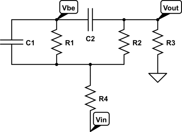
schematic

simulate this circuit – Schematic created using CircuitLab

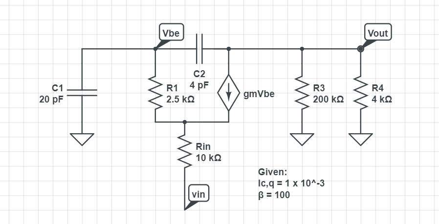
I've been scratching my head with this one. The circuit below is a small signal equivalent circuit of a PNP CB amplifier. I'm trying to get the transfer function Vout/Vin. I was already able to find Vout/Vbe using KCL across the node Vout. Now i'm stuck with the equation for Vin. Could anybody help me get started?

Here is what I got for Vout/Vbe where Rout = R3//R4:

$$\frac{v_{out}}{v_{be}}= \frac{g_{m}R_{out}*1-\frac{sC_{2}}{g_{m}} }{1+sR_{out}C_{2}} $$

Edit: I made quite the mistake in the schematic.

Edit(2): Here is the old schematic:

enter image description here

\$\endgroup\$
3
  • \$\begingroup\$ What KCL equation have you written for the node at the junction of Rin, R1 and gmVbe ? Eliminate Vbe from that node equation using the vout/vbe transfer function. \$\endgroup\$
    – AJN
    Commented Jan 31, 2021 at 15:07
  • \$\begingroup\$ @AJN Wouldn't that node be Ve? But i don't know what Ve is. Or would it be Veb? Not really sure. \$\endgroup\$
    – user266967
    Commented Jan 31, 2021 at 15:15
  • \$\begingroup\$ For a CB configuration C1 would always be a lot bigger than C2 so that would simplify things a bit. I'm saying this because any simple model of a BJT is going to be no better than 70% accurate. Also, you have Vbe on a node but that node is the base. The emitter should be the north side of Rin as far as I can tell. \$\endgroup\$
    – Andy aka
    Commented Jan 31, 2021 at 15:22

1 Answer 1

2
\$\begingroup\$

How do I get a KCL equation involving Vin in this circuit?

KCL equations involve currents, not voltages, that said this might be the answer you are looking for..

In the case of your circuit there is only one KCL equation which can be made to involve \$ Vin \$, namely the sum of the currents into the node between \$ R1 \$, \$ Rin \$ and the current source: \$ I_{R1} + I_{Rin} + gm V_{be} = 0\$ (1)

now from ohm's-law; \$ I_{R1} = \frac{V_{R1}}{R1} \$ (2) and \$ I_{Rin} = \frac{V_{Rin}}{R_{in}} \$ (3)

substituting (2) and (3) into (1); \$ \frac{V_{R1}}{R_{1}} + \frac{V_{Rin}}{R_{in}} + gm V_{be} = 0 \$ (4)

to get \$ V_{in} \$ involved we can apply KVL to the mesh involving the voltages across the two resisors; \$ V_{in} - V_{Rin} + V_{R1} - V_{be} = 0 \Leftrightarrow V_{in} + V_{R1} - V_{be} = V_{Rin} \$ (5)

substituting (5) into (4); \$ \frac{V_{R1}}{R_{1}} + \frac{V_{in} + V_{R1} - V_{be}}{R_{in}} + gm V_{be} = 0 \$ (6)

And now you have a KCL equation (6) involving \$ V_{in} \$

Here the reference directions are taken such that all currents into the node are possitive, and the voltage reference directions follow from the standard conventions.

EDIT; The OP made a mistake in the schematic,

after the correction equation (1) has to be; \$ I_{C1} + I_{R1} + I_{Rin} + gm V_{be} = 0\$ (1b)

and equation (6) becomes; \$ I_{C1} + \frac{V_{R1}}{R_{1}} + \frac{V_{in} + V_{R1} - V_{be}}{R_{in}} + gm V_{be} = 0 \$ (6b),

to find \$ I_{C1} \$ we need to use that; \$ I_{C1} = C_1 \frac{d}{dt} V_{C1} \$ (7),

since \$ V_{C1} = V_{R1} \$ (8) substituting (8) into (7) we can write this as; \$ I_{C1} = C_1 \frac{d}{dt} V_{R1} \$ (9).

substituting (9) into (6b) yields; \$ C_1 \frac{d}{dt} V_{R1} + \frac{V_{R1}}{R_{1}} + \frac{V_{in} + V_{R1} - V_{be}}{R_{in}} + gm V_{be} = 0 \$ (10)

or if you want the solution in the laplace/s -domain; \$ s C_1 V_{R1} + \frac{V_{R1}}{R_{1}} + \frac{V_{in} + V_{R1} - V_{be}}{R_{in}} + gm V_{be} = 0 \$ (10b).

Comment; Please do not remove your previous picture etc, but add the new one as an edit!
\$\endgroup\$
7
  • \$\begingroup\$ Thanks! I understand your solution but I actually made quite the mistake in my presented schematic which I have corrected now. C1 wasn't suppose to be grounded. How would C1 appear in the equation with Vin? Should I just add the current flowing through C1 as Ic1 = Vbe*sC1 in the sum of currents equation? \$\endgroup\$
    – user266967
    Commented Jan 31, 2021 at 19:02
  • 1
    \$\begingroup\$ @Rein I have updated my answer to reflect your correction, please do not remove your old scematic but add the new one as an edit!!! \$\endgroup\$
    – user173292
    Commented Jan 31, 2021 at 19:19
  • \$\begingroup\$ Thanks so much! I will bring back the old schematic too! \$\endgroup\$
    – user266967
    Commented Jan 31, 2021 at 19:33
  • \$\begingroup\$ I noticed that you had Vbe and Vr1 as two different voltages. Shouldn't they be the same? \$\endgroup\$
    – user266967
    Commented Jan 31, 2021 at 19:42
  • 1
    \$\begingroup\$ @Rein No they should not be the same, V_be is a node voltage compared to GND where as V_r1 is the voltage across R1.. \$\endgroup\$
    – user173292
    Commented Jan 31, 2021 at 19:43

Your Answer

By clicking “Post Your Answer”, you agree to our terms of service and acknowledge you have read our privacy policy.