6
\$\begingroup\$

I am working on a design for a high-speed data acquisition device for a 10-bit ADC signal at 80 Msps. So far, it looks like most MCU boards are too slow to be able to route and store data and keep up with the high sampling rate. The latest board that I've been looking at is the Teensy 4.1 with a CPU frequency of 600 MHz (can go higher with overclocking, up to ~1 GHz with cooling). What I am wondering is if I can circumvent this issue by interfacing the ADC output directly with the I/O pins on a memory IC or SDRAM chip. In this scenario, I would use the Teensy 4.1 to drive the clock signals and logic signals for both the ADC and SDRAM.

In order to read the data from the SDRAM, I would use a multiplexer to re-route the I/O pins on the SDRAM to the Teensy 4.1, which can process the data and write it to external memory via SDIO. The multiplexer would only be used to switch the signals after my measurement is complete.

I've included a schematic below for what I am trying to describe above. Is this something that can physically be done?

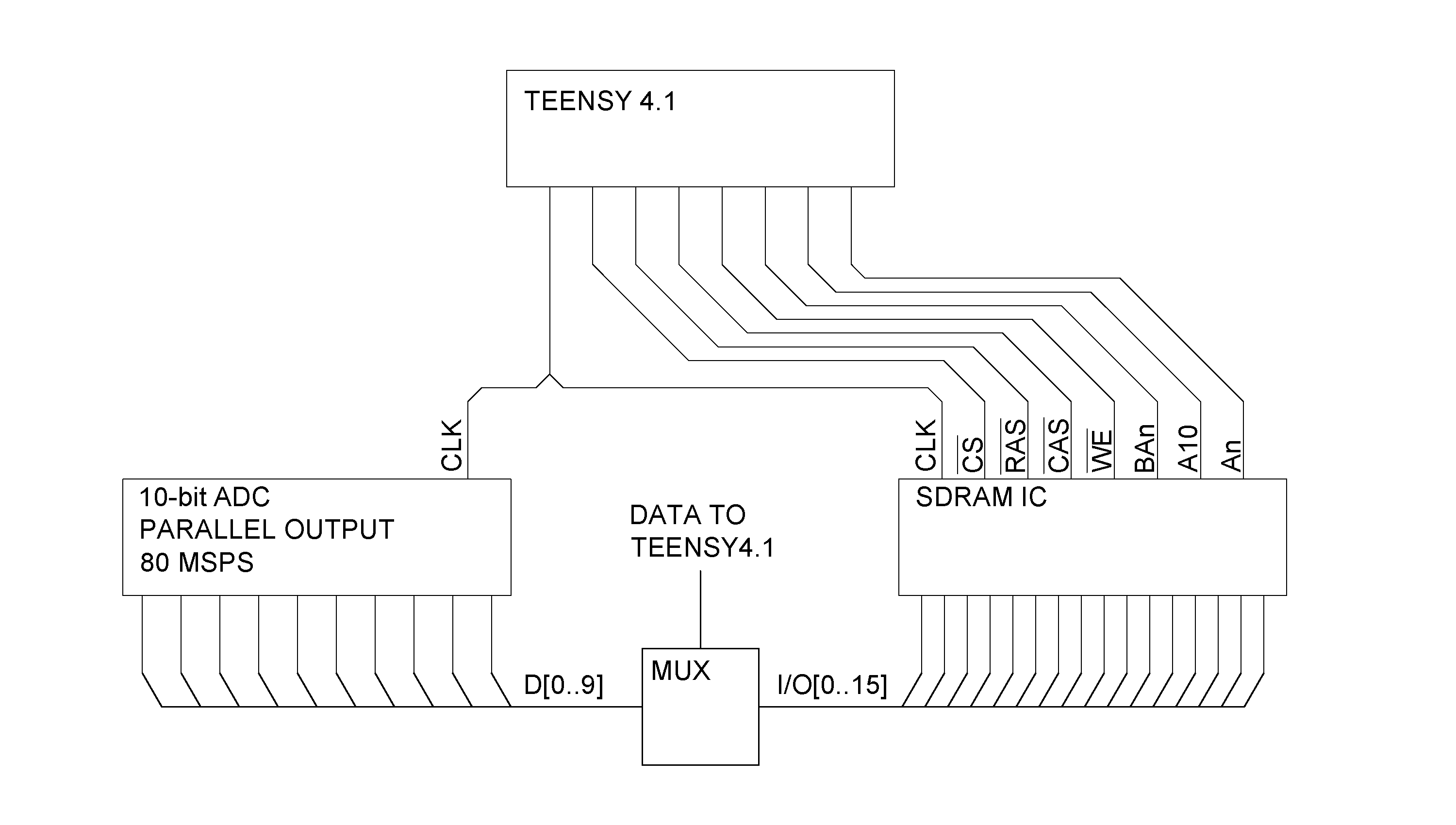
enter image description here

\$\endgroup\$
6
  • 3
    \$\begingroup\$ Using DMA might also be an option... \$\endgroup\$
    – Sim Son
    Feb 6, 2021 at 18:48
  • \$\begingroup\$ community.nxp.com/t5/i-MX-RT/RT1064-ADC-ETC-with-DMA/m-p/852351 \$\endgroup\$ Feb 6, 2021 at 19:11
  • 7
    \$\begingroup\$ This is a good job for an FPGA. \$\endgroup\$
    – user16324
    Feb 6, 2021 at 19:31
  • 1
    \$\begingroup\$ How much data do you intend to record? 64 kilobytes ought to be enough for anybody, but sometimes it's not. If you answer "unlimited" then do you want to stream it over USB3.0, Gb Ethernet, pci-express, or "other"? Or, do you want to record it to flash, SD card, eMMC, etc? (80 Msps is a bit extreme for SD card though) Also if you answer "more than a megabyte", how much do you love BGA packages? \$\endgroup\$
    – bobflux
    Feb 6, 2021 at 19:38
  • 1
    \$\begingroup\$ What's the ultimate destination for the data? USB asic would cost a few tens of dollars and can trivially do such data rates, but that assumes your goal is to get data to a PC. \$\endgroup\$ Feb 6, 2021 at 20:20

4 Answers 4

8
\$\begingroup\$

In principle, this looks like of especially older acquisition devices worked.

Practically, you're still facing a few core problems with your SDRAM:

  1. It's non-trivial to work with SDRAM; you must make sure that for the duration of your acquisition, you can count up addresses at 80 MHz, as well as that the SDRAM is able to accept new data every clock. Usually, that's not the case, with finite burst sizes, and with refresh cycles that need to be inserted. SRAM might be easier to deal with
  2. Your Teensy still has to generate 80 million addresses a second, far as I can tell, or if you can program the SDRAM into accepting bursts of length larger than a word, a factor of that.

Honestly, this sounds a lot like you want SRAM in this application, not SDRAM, and the clock speed sounds like Pseudo-SRAM would do.

You'd also want to find an easy way to implement your mux, and while you're at it, solve the address generation timing problem, as well as reliable clock generation.

Honestly, this all sounds like a small FPGA in the middle would do much better:

      10b       2×8b data
ADC ==//==>FPGA====//====>PSRAM
           ||   x b addr  ^ ^
           \\======//====// |
           |      clk       |
           \------//--------/

Implementing an address counter in an FPGA is pretty straight forward, and having that FPGA allows you to handle, delay, scale, encode your ADC data on the fly.

For reading from a host MCU, an SPI interface would be pretty straightforward to have in the same FPGA, allowing you to keep the PCB complexity at bay.

Which FPGA? Don't know, it doesn't have to be large, and if you use one of the lower-pin-count PSRAMs (I've never worked with them, but I find Infineon HyperRAM quite interesting), you don't need more than maybe 32 IO pads; a medium-sized Lattice ICE40 might do (and there's an open source toolchain to produce FPGA images, which is a big plus in terms of vendor freedom).

Addition: Oh, scratch the HyperRAM. I've miscalculated: you need to sustain a 800 Mbps write rate. The interface of that device class will not do that.

\$\endgroup\$
8
\$\begingroup\$

What you are describing is a direct memory access (DMA) operation.

It looks like the Teensy 4.1 uses an NXP MIMXRT1062 processor, and that processor does have a DMA engine -- but in order to work for you that DMA engine would have to work with parallel data in, and would have to be otherwise compatible with the ADC you're proposing to use. Unless there's something already in the Teensy ecosystem that supports it, you're going to have a long uphill battle to make it work.

(n.b: See Dave Tweed's answer pertaining to the CMOS Sensor Interface -- if you can make that work it should have more than enough speed.)

To put the above statement into perspective: I've been doing this stuff for 30 years now; if my boss came into my cubicle right now (oh, COVID, when will you be done?) and asked me how long it would take I'd say "I've just spent 60 seconds skimming the datasheet, and the chip has DMA -- at minimum, a month; at maximum, maybe never.

So -- dig in to the datasheet, find a Teensy forum to ask your question, and start learning a lot.

If you can't do this using the processor's DMA, then your best bet if you want to use the Teensy is to use a CPLD from Lattice or Xilinx or whoever plus an external RAM chip that handles the DMA for you, and lets you access the memory from the Teensy. This will be an even longer steeper uphill battle.

If you can't use the processor's DMA and you're willing to give up on using the Teensy, then your best bet overall may be to get dev board for an FPGA with an embedded processor (like Xilinx's Zynq), and do it all there. If I'm correct about your abilities this will be your longest and steepest uphill battle, but when you're done you'll have a board with an ADC mezzanine board (or even built in -- some of the Zynq dev boards come with ADCs) instead of a Teensy with all sorts of crap glommed onto it.

\$\endgroup\$
2
  • \$\begingroup\$ Thank you Tim! You're correct on the DMA for that processor, but in the Teensy forums, users have found it frustrating to work with. The DMA doesn't actually interface with the fastest GPIO pins, so it's limited to a low input rate. The four fast GPIO pins (running at CPU clock) can really only do direct to memory, which is still slow. I've been nervous to jump into FPGA as I don't even have much experience with MCUs, but it's looking like that's my best route to follow for what I'm trying to do \$\endgroup\$ Feb 7, 2021 at 20:15
  • 2
    \$\begingroup\$ You missed the CSI (CMOS Sensor Interface) module, which is specifically designed to capture parallel data of up to 24 bits at up to 80 MHz. It's perfect for this application. \$\endgroup\$
    – Dave Tweed
    Feb 14, 2021 at 13:28
3
\$\begingroup\$

"64 kB ought to be enough for anybody" so why not use a FIFO chip?

It has all the built-in counters and logic, it will take your ADC data and store it, then deliver it later to the micro at a pace of your choosing. But, of course, it's only 64kB and sells for the price of a 16GB DDR4 stick. And it's pretty oldskool.

The Teensy uses a slow QSPI RAM chip that won't be able to record at 10 bit 80Msps. So you'd be limited to the micro's internal RAM.

Now in the LPC43xx microcontroller family there is one with a 80Msps ADC. It's inside the micro, so you don't need to worry about layout and high speed clocks, which is a plus. These chips also have massive memory bandwidth and a DMA controller that really rips, but the internal memory is limited at 204 kB. They do have a SDRAM controller though.

One nice solution would be to find a readymade board with a micro that has a high-speed ADC and a SDRAM chip (a real one, not SPI).

\$\endgroup\$
3
  • \$\begingroup\$ Nice answer! Heads up though: Cypress/Infineon have –I cite– "pruned" their FIFO products completely: cypress.com/products/fifos \$\endgroup\$ Feb 6, 2021 at 20:20
  • \$\begingroup\$ Ah, so that's why it was cheaper than the others on digikey -- well, there are other manufacturers, more expensive of course \$\endgroup\$
    – bobflux
    Feb 6, 2021 at 20:37
  • \$\begingroup\$ yeah, welcome to the world of products that CPLDs and FPGAs have made harder to obtain :) On the other hand, pretty cool that you can build a FIFO like that with a 3€ FPGA \$\endgroup\$ Feb 6, 2021 at 20:37
0
\$\begingroup\$

The i.MX RT1060 processor used on the Teensy 4.1 is perfectly capable of handling your 80 MHz, 10-bit parallel data all by itself. There's no need to mess around with external memory, especially SDRAM.

The 3437-page reference manual (additional documentation here) for this chip is quite daunting, but take a look at chapter 34, "CMOS Sensor Interface" — specifically, section 34.5.3 ""Non-Gated Clock Mode", which explains how to capture large frames of data.

I doubt that you're going to find much in the way of preexisting library code for this peripheral, so you're going to have to get down-and-dirty with programming it yourself. You'll also need to get familiar with the Clock Controller Module (chapter 14).

\$\endgroup\$

Your Answer

By clicking “Post Your Answer”, you agree to our terms of service and acknowledge that you have read and understand our privacy policy and code of conduct.

Not the answer you're looking for? Browse other questions tagged or ask your own question.