0
\$\begingroup\$

I'm in front of a big question. I need to route 90 Ohms differential lines for a USB 2.0 Project.

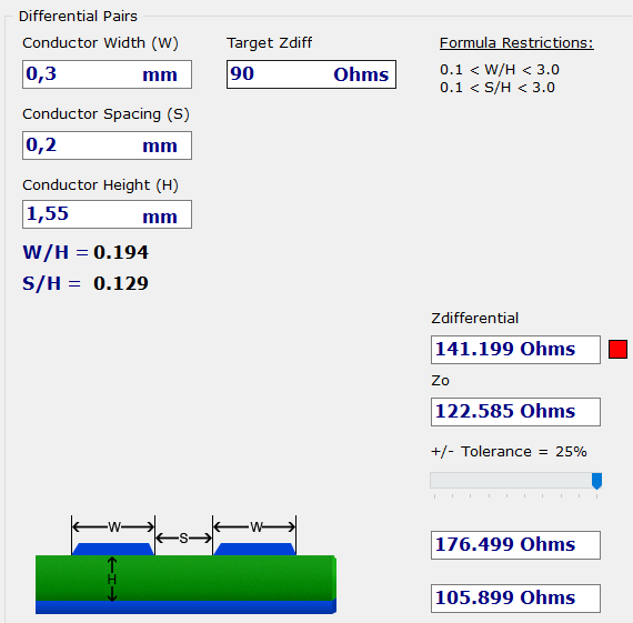
I understand how to use tools like Saturn PCB Design to give me the correct spacing and lines width.

enter image description here

But it seems difficult to achieve fabrication constraints, for example with Eurocircuits :

enter image description here

I can't route these lines with basic technology settings (0.15mm) ? Although i can route larger lines, i can't use >1mm widths on some integrated circuits.

Thank's to help me to understand how to achieve the best compromise between pcb layout constraints and signal integrity requirements.

Adrien

\$\endgroup\$
2
  • \$\begingroup\$ I don't understand what your actual question is. \$\endgroup\$
    – Andy aka
    Commented Feb 8, 2021 at 10:46
  • \$\begingroup\$ Which flavor of USB 2 do you use? full speed or high speed? \$\endgroup\$
    – asdfex
    Commented Feb 8, 2021 at 11:33

1 Answer 1

2
\$\begingroup\$

The only parameter you can change to solve this is the substrate height. Either use a thinner PCB or if that is not enough to get sufficiently narrow lines, place a ground plane below the trace - this means you need a multi layer PCB. Check if they will guarantee the impedance (material selection and actual stack-up). If not, this may require you to request a controlled impedance production which of course will be more expensive.

\$\endgroup\$
4
  • \$\begingroup\$ We always allow the PWB vendor to adjust things like trace width, separation, and height as needed to meet their manufacturing guidelines and give us a good product yield, and still meet the parameters we care most about like Zo. We stay in the loop with the vendor and need to approve any such deviations from the routing guidelines we provide to them. \$\endgroup\$
    – SteveSh
    Commented Feb 8, 2021 at 12:30
  • \$\begingroup\$ @SteveSh This is one approach. This will likely fail in the case described in the question, because it is impossible (within reasonable trace widths) to achieve the requested impedance without changing the PCB thickness or add a GND layer. Both very significant changes which only the designer should alter. \$\endgroup\$ Commented Feb 8, 2021 at 16:31
  • \$\begingroup\$ OP has specified a height of 1.5 mm, which is 60 mils, which paints him into a "can't get there from here" corner, as you pointed out. That's way out of line by today's standards. We can do a whole 10 layer board in 60 mils, with most of heights above a reference plain around 5 mils. If he made his H 0.15 mm, he'd be a lot closer \$\endgroup\$
    – SteveSh
    Commented Feb 8, 2021 at 19:46
  • \$\begingroup\$ It's a typical problem. Usually USB lines are used in 4 layer boards (for many many reason), so the reference plane is nearer (depending on your stacking). If you are using USB 1 (12Mb/s) you could deviate slightly (to the limit of your fabrication), keep the track shortest as possible and hope all goes well. Doing high speed USB2 on two layer is IMHO quite challenging (also: substrate is quite variable) \$\endgroup\$ Commented Feb 8, 2021 at 20:35

Your Answer

By clicking “Post Your Answer”, you agree to our terms of service and acknowledge you have read our privacy policy.

Not the answer you're looking for? Browse other questions tagged or ask your own question.