1
\$\begingroup\$

I try to program a design I made using 5M40ZE64C5N CPLD. The software side was successful and I got a .pof file without any critical warnings or errors. The problem occurs when I try to upload the design to real hardware using USB-blaster by JTAG. It doesn't work completely. I followed this diagram: enter image description here

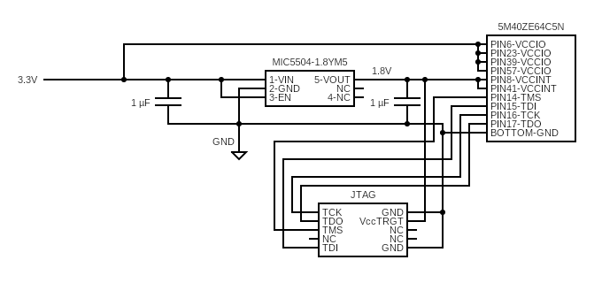
The JTAG connections to CPLD are like from this picture and go to CPLD corresponding pins 14-17. I connect GND to board GND and VTref to VCCINT (1.8V). I also connect power pins 3.3V and GND to Arduino UNO clone. There is only 5M40ZE64C5N chip, 3.3V -> 1.8V voltage regulator and 2x 1uF caps on this board at this moment and absolutely nothing else

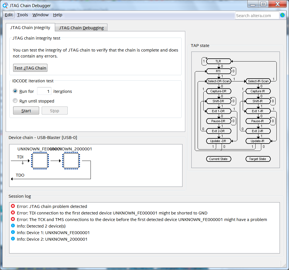
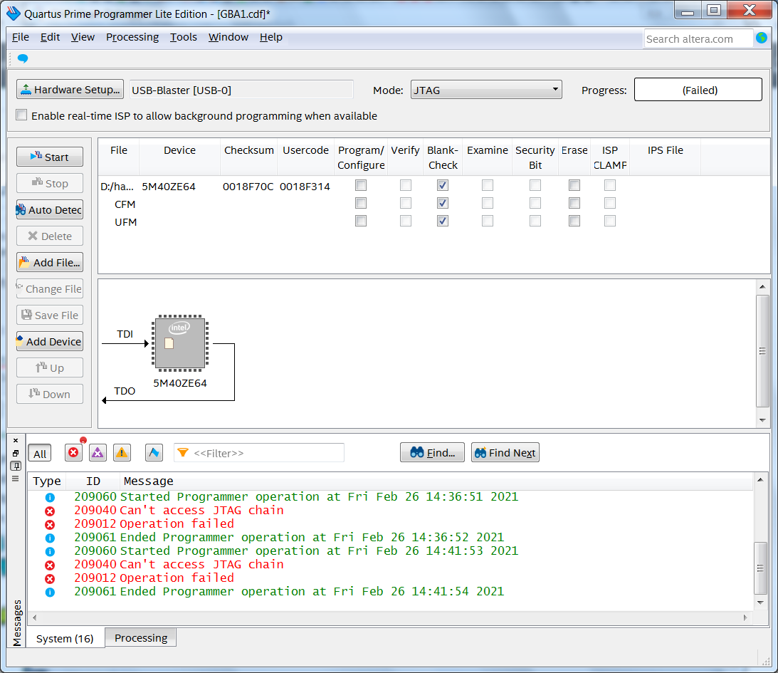
As I said, the board doesn't work at all. Quartus throws "Can't access JTAG chain" error. However once I try to run JTAG debugger then things get interesting- it detects 2 devices instead of 1. Here are full logs:

Info (209060): Started Programmer operation at Fri Feb 26 14:41:53 2021
Error (209040): Can't access JTAG chain
Error (209012): Operation failed
Info (209061): Ended Programmer operation at Fri Feb 26 14:41:54 2021


!Error: JTAG chain problem detected
!Error: TDI connection to the first detected device UNKNOWN_FE000001 might be shorted to GND
!Error: The TCK and TMS connections to the device before the first detected device UNKNOWN_FE000001 might have a problem
!Info: Detected 2 device(s)
!Info: Device 1: UNKNOWN_FE000001
!Info: Device 2: UNKNOWN_2000001

When I check connections with multimeter, nothing is shorted to GND, VCC, together or anywhere else where it was not supposed to be. The chip was soldered using hot air and looks fine. Everything looks like the cleanest job ever with best connections but it doesn't work. 3 different PCBs show the same exact result. Please give me some advices because it starts to drive me crazy... Many thanks in advance! enter image description here enter image description here
UPDATE: here's the diagram of the essential section. There is nothing else on this board anyway at this moment enter image description here
\$\endgroup\$
4
  • \$\begingroup\$ There is an issue with your board or programmer. Possibly a short, possibly you're using the wrong voltage, possibly you've missed a pull-up resistor on some configuration pin somewhere. However as you haven't shared any photos or diagrams of your circuit and schematic, there is little we can do to help \$\endgroup\$ Commented Feb 26, 2021 at 14:25
  • \$\begingroup\$ Uploaded the schematic now \$\endgroup\$ Commented Feb 26, 2021 at 15:10
  • \$\begingroup\$ Per this, the TCK needs a 1k pull down. TMS and TDI need 10k pull ups to VCCIO1. \$\endgroup\$ Commented Feb 26, 2021 at 15:40
  • \$\begingroup\$ Furthermore, your VccTRGT for the JTAG header should be to 3.3V as all of your VCCIO pins are driven at 3.3V \$\endgroup\$ Commented Feb 26, 2021 at 15:40

2 Answers 2

2
\$\begingroup\$

Your main issue is that you are running your JTAG header at the wrong voltage. Your VCCIO pins are connected to 3.3V, which means the JTAG signalling level is set to 3.3V

However, on your JTAG header, you have fed 1.8V to the VCCTrgt pin, which means that the JTAG programmer is trying to run at 1.8V. The signals are therefore getting corrupted because the programmer cannot drive the TDI, TMS nor TCK lines to a sufficient logic level for the Max V to read them.

Routing 3.3V to the VCCTrgt pin should largely solve the problem.

Furthermore, per the pin configuraiton guidelines for the Max V, you are missing necessary resistors on the JTAG lines. The TCK needs a 1k pull down to GND. TMS and TDI need 10k pull ups to VCCIO1.

\$\endgroup\$
1
\$\begingroup\$

Well it looks like I kinda answered my own question. I don't know where but I read somewhere, in some manual that VccTRGT needs to be connected to VCCINT while this manual clearly states otherwise. The VccTRGT should be connected to VCCIO instead: https://www.intel.com/content/dam/www/programmable/us/en/pdfs/literature/hb/max-v/mv51006.pdf

You can program MAX V devices by downloading the information through in-circuit
testers, embedded processors, the Altera® ByteBlaster™ II, EthernetBlaster II,
EthernetBlaster, and USB-Blaster™ cables. You need to power up these cable’s
VCC(TRGT) with VCCIO of Bank 1.

Once I connected VccTRGT to VCCIO (3.3V in this case), it worked! Many thanks for your suggestions!

\$\endgroup\$

Your Answer

By clicking “Post Your Answer”, you agree to our terms of service and acknowledge you have read our privacy policy.

Not the answer you're looking for? Browse other questions tagged or ask your own question.