15
\$\begingroup\$

I'm trying to restore and learn from a simple metronome assembled by my uncle in the 60's. It has a nice sounding beat and used to work until very recently — although unstable. I've made a schematic from tracing the board tracks which is included below without the power supply for simplicity.

Being a beginner myself, I cannot understand the disposition of Q1 and Q2. It looks like the SCR explanations I've seen around, but I'm not really sure if they are there to work as an SCR.

I assume that the rightmost part with Q3 and Q4 is just there to amplify a pulse generated by the leftmost part of the circuit, specifically coming from between R4 and C2. But how does this oscillator work at all?

The transistors are from RCA, with SK3020 being a silicon NPN and SK3005 actually a germanium PNP. I'm not sure if there are any particular characteristics of them that enable this functionality, and I could not find much about their differences to modern silicon transistors.

Any pointers or topics to read about in the direction of understanding how this circuit is creating pulses is greatly appreciated.


Notes:

  • Added the voltages I'm reading now throughout the circuit.
  • The circuit was recognized by Spehro Pefhany as part of the RCA Hobby Circuits Manual, 1968, the original circuit is included in his answer.

Metronome Electronic Circuit

\$\endgroup\$
4
  • \$\begingroup\$ Modify schematic with voltages to diagnose error. Caps maybe leaky \$\endgroup\$
    – D.A.S.
    Commented Feb 26, 2021 at 16:28
  • 3
    \$\begingroup\$ Q1/Q2 form a composite silicon-controlled-rectifier (SCR), although this one is germanium. I would suggest that generic silicon transistors could likely be substituted, and it would still work. \$\endgroup\$
    – glen_geek
    Commented Feb 26, 2021 at 16:49
  • \$\begingroup\$ @TonyStewartSunnyskyguyEE75. Done. Thank you! \$\endgroup\$
    – sidyll
    Commented Feb 26, 2021 at 16:51
  • 2
    \$\begingroup\$ Q4 is definitely busted if it has 11.7 volts on the base. For the same reason, so is Q2. \$\endgroup\$
    – Andy aka
    Commented Feb 26, 2021 at 17:44

6 Answers 6

14
\$\begingroup\$

Q2 is a ramp retrace generator.
Q1 is a reset comparator when it’s Vbe >200 mV for Germanium. But if Q2-C is low, and Q1-E is high , Q1 is defective due Q1 Vbe defect.

Now I see Q2 & Q4 Vbe >1V are both defective

enter image description here

Theory of Op.

This is a clever little 2 transistor Astable multivibrator with a pulse generator to drive the speaker with a spike from 1/4 or 1/2s to 2s for a metronome like click generator with RV1. Beyond this range it stops to oscillate due to gain ratios of Rc/Re.

The Sawtooth Generator ramps up Q2's emitter cap. initially but then has little effect after that on frequency as Q1 effectively cuts off Q2 from conducting current by pulling the emitter voltage up far above the base voltage. In fact too far as Q2’s Vbe > -5V which is a common MUST NOT EXCEED rating for most transistors.

Once Q2's current ramp reaches it's Vbe threshold of ~ 100mV for Ge or 600 mV for Si, Q1 then fires the SCR trigger and pulls up Q2.

R3 then pulls down the cap voltage until Q2 can conduct and is triggered then by the positive feedback loop (SCR like effect) of Q1 to Q2 with Q1-Vbe being the comparator and Q2 being the discharge which turns itself off by the R ratio of R6 being much smaller than Q2 emitter R.

R1,R2 and Q2 emitter-follower is only to set the sawtooth to the low voltage < 1/3 of 12V Then R4 pulls up the voltage too high, so I would increase it and at the same time R1,R2 to reduce excess power consumption of the bias to Q2.

My recommendations are on the mark-up schematic. But mainly since Ge transistors are rare, change Q1 to any Si PNP and R6 to 5.6k and replace dead Q2,Q4 with PN2222A or equivalent.

Root Cause Failure Analysis

  1. Q2 and Q4 have fused open Base Emitter junctions
  2. Veb reverse voltage exceeds 5V slightly causing slow damage to junction while R4 is drives Q2 hard on reset stressing the junction again with more than 50mA.
  3. Q4 also has high base current and when blown, R8 gets warm.

Fun fact: the two transistors look like an SCR, but is not since there are 4 terminals unlike an SCR which exposes only 3 terminals. The 4th is used for biasing both off and detect the current in R6 until the top one conducts and is reamplified with positive feedback from the lower Q2 to rapidly switch for the sharp edge of the sawtooth. Then they both shutoff as the RC circuit decays with a linear ramp then repeats.

\$\endgroup\$
14
  • \$\begingroup\$ Thank you very much! The hard part is choosing the accepted answer… Your idea of measuring voltages never occurred to me (sorry, I'm still learning) but immediately made me conclude while measuring that these components were faulty. I also noticed R8 is heating up a little and is probably in bad shape too, since it's not conducting at all. In an attempt to restore this 50+ y.o. device I'll try my best to find these components to replace. I can't thank you enough, just learned a lot! \$\endgroup\$
    – sidyll
    Commented Feb 26, 2021 at 17:26
  • \$\begingroup\$ I know how to explain it better, why it worked and how to fix it ,so don't be too quick \$\endgroup\$
    – D.A.S.
    Commented Feb 26, 2021 at 17:48
  • \$\begingroup\$ Sir, I can't thank you enough for your in-depth analysis and explanation. Some details which I'd like to add are: (1) after the astonishing discovery by @Spehro Pefhany below regarding this circuit being part of a manual by RCA, I noticed the original uses 9V instead of 12V. This probably played a role in the cumulative damage to such components. Unfortunately the memory of why my uncle chose to use that is lost in the memory, just like how would this circuit arrived in my country so early (specially during a period of dictatorship). I think this will remain a mystery. \$\endgroup\$
    – sidyll
    Commented Feb 27, 2021 at 3:27
  • \$\begingroup\$ (2) I managed to find some old stock of both transistors in a shop. Thanks to your guidence I will restore this device for historic reasons as well as building a new one adapted to modern transistors. \$\endgroup\$
    – sidyll
    Commented Feb 27, 2021 at 3:28
  • 1
    \$\begingroup\$ archive.org/details/rcasolidstatepow00rcac/page/196/mode/… most of the analog type questions for EE's were done in the late '60's and answered in this book which can be rented for 1 hr free \$\endgroup\$
    – D.A.S.
    Commented Feb 27, 2021 at 20:50
15
\$\begingroup\$

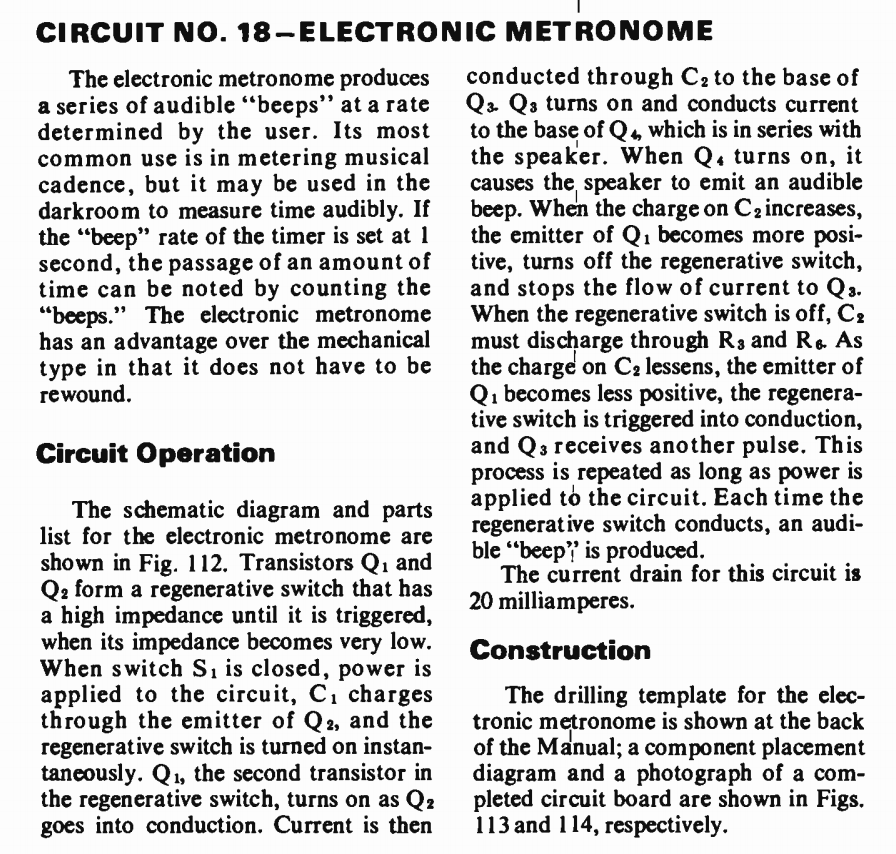
This circuit was copied out of the RCA Hobby Circuits Manual 1968. Complete entry shown below, including original description of operation.

enter image description here

enter image description here

\$\endgroup\$
4
  • \$\begingroup\$ Wow, I'm surprised! Thank you very much! I have no idea how this circuit could have traveled overseas on that date, but it sure did. I modified the question to credit it appropriately. Thank you for recognizing and providing this such a valuable and enlightening information. \$\endgroup\$
    – sidyll
    Commented Feb 27, 2021 at 3:20
  • \$\begingroup\$ This is the same circuit but doesn't have the same flaw of excess Veb on Q2 because the V+ is only 9V instead of 12V so 9V is safer \$\endgroup\$
    – D.A.S.
    Commented Feb 27, 2021 at 4:53
  • \$\begingroup\$ However R3 (or R2 here) is still a problem with driving almost 100mA base current in Q2 . But Sphero, this design is not dependent on hFE which only affects the cap discharge risetime and not the ramp. R3 & Pot control the ramp with C. R3 is more likely to cause latchup and Rc/Re ratio for Q2 \$\endgroup\$
    – D.A.S.
    Commented Feb 27, 2021 at 5:16
  • \$\begingroup\$ @TonyStewartSunnyskyguyEE75 Yes, I think you're right. It's biased so that it has to turn off. \$\endgroup\$ Commented Feb 27, 2021 at 5:29
9
\$\begingroup\$

To answer the question you didn't ask:

In normal operation, with the transistor on, the base-emitter voltage of a bipolar junction transistor is about one diode drop. That's 0.7V for a small-signal silicon transistor (it can be more if the thing's carrying huge currents), and about 0.3V for a small-signal germanium transistor.

The direction of the voltage is base positive for an NPN, base negative for a PNP (it follows the 'P' and 'N' in the name).

If you see more than that, the transistor is broken. If you see less, either the transistor is broken or it's turned off (which can be the case for this circuit: in normal operation Q1 and Q2 will almost never be on at the same time). Since this circuit is designed to be an oscillator, you can't just measure voltages statically -- trying would just get you messed up measurements because the voltages would be bouncing around. However, if you put one meter lead on the base and the other on the emitter and measure there, then you'll always be measuring the voltage of interest.

Note that you could have a cracked PCB, in which case you can't assume that the voltage on the transistor lead is the same as the voltage on the PCB trace.

If your measurements are correct, you've got 10V across the B-E junction of Q2, and 11.7V across the B-E junction of Q4. Unless lightning struck the thing (or a cat peed in it a year ago and it corroded, or some other disaster struck) it's unlikely that two transistors broken at once. I'd re-measure just across those junctions and see if you're getting consistent readings.

\$\endgroup\$
7
  • \$\begingroup\$ Some assumptions are not validated, when the circuit is stressing Q2 Veb from R4 which was the main fault in the design. Then when Q2 failed, R4 then sustained excess base current in Q4. \$\endgroup\$
    – D.A.S.
    Commented Feb 26, 2021 at 19:01
  • \$\begingroup\$ Thank you for answering what I didn't ask but should have :) The PCB seems to be perfect. If I may comment on something, I was wondering if the circuit being in "operation" as referred means functional. I had some trouble interpreting. Further, in the last sentence of the 3rd paragraph such measurement should be made with the transistor removed from the board, correct? Maybe a newbie question but I thought I should ask. Anyway, with Q2 removed, the BE junction doesn't even ready anything on my multimeter (stays at 1) which might be indeed proof of its malfunction. \$\endgroup\$
    – sidyll
    Commented Feb 27, 2021 at 3:02
  • \$\begingroup\$ As for damage, taking a second look I can see that this was mounted pretty close to the power supply which itself is build on one of those old terminal strips. Not only I don't trust it, having it eventually touching one of the transistor cases is a not unlikely — also considering it's all mounted on a cardboard box. Well crafted, but not the most sturdy material. Other than that, Tony's analysis does prove some dimensions are off and the discovery of the original circuit also shows 12V is incorrect. \$\endgroup\$
    – sidyll
    Commented Feb 27, 2021 at 3:12
  • \$\begingroup\$ You definitely want to do your measurements in-circuit, with things turned on. I.e., "in operation" means you waltz up to the thing with power turned on and a multimeter in hand, and take some measurements. Without current applied, the voltages across the transistor leads should be zero (unless the world has suddenly gotten very weird). \$\endgroup\$
    – TimWescott
    Commented Feb 27, 2021 at 3:29
  • \$\begingroup\$ I edited this, hopefully for clarity. I realized I was using "operation" with two different meanings in two different places -- and you're a newbie. Bad me. \$\endgroup\$
    – TimWescott
    Commented Feb 27, 2021 at 3:40
4
\$\begingroup\$

It does work like an SCR as you described.

Assume C3 is charged to a higher voltage than the junction of R1 and R2 (about 4V).

C3 discharges through R5 and RV1 relatively slowly creating an exponential negative going ramp until the voltage becomes slightly lower than 4V; Q2 will then start conducting. The current from Q2 through R6 will forward bias Q1 that will then raise the voltage of Q2 base causing it to conduct more.

This proceeds until both Q1 and Q2 are conducting heavily and charging up C3.

As C3 charges, the current into the base of Q1 reduces until it is insufficient to keep Q2 conducting and the process stops with neither Q1 or Q2 conducting and C3 charged up close to 12V. C3 will then discharge through R5 and RV1 to start another cycle.

This sequence will result in a continuous sawtooth waveform across C3 with short pulses of current through Q1 and Q2.

If you replace the transistors with silicon ones R6 will need to be increased greatly because of the higher Vbe of silicon transistors (Maybe to 220k, it would work even without a resistor at all).

As you correctly state the remainder of the circuit is to amplify the pulse from Q1 to a level suitable to drive a speaker.

As @Tony Stewart mentions in the comments leakage in the capacitor C3 could stop the circuit from working or make it unstable.

\$\endgroup\$
2
  • \$\begingroup\$ This does not explain how the sawtooth generator works , why it failed or how to fix it and what was wrong with the design \$\endgroup\$
    – D.A.S.
    Commented Feb 26, 2021 at 17:47
  • 1
    \$\begingroup\$ The only error in your description is the precise requirement for R6 which must match the threshold voltage of Q1 -Vbe for the ratio of Rv1/R6 from 2 to 5 or so for Si and 12 to 30 for Ge due to Vcc and Vbe ratio and limited range of metronome from 1/4 beat to full beat (-1) otherwise OK \$\endgroup\$
    – D.A.S.
    Commented Feb 26, 2021 at 18:41
2
\$\begingroup\$

Regarding your intent to use germanium and silicon transistors:

The circuit can pretty much work with whatever silicon transistors you build it, as long as you don't mistake pnp for npn ones.

The reason why PNP ones are germanium and NPN ones are silicon lies in the history of the semiconductor technology. It is easier (i.e. cheaper) to make NPN silicon transistors (starting from low-doped N bulk silicon) and it is easier to make PNP germanium transistors. That's why older (germanium-era) circuits tend to use more PNP transistors and newer circuits lean to NPN. Your metronome is in the middle with equal number of both.

Regarding the unstable work of the metronome:

Capacitors dry up, variable resistors flake their resistive layer. The circuit uses C3 and R5 + RV1 to set the pulse timing.

C3 is electrolytic and prone to drying of the electrolyte (making it unstable long term and depending on temperature),

RV1 is a variable resistor that wears out and gets unstable short term (up to changing its value significantly because of a speaker vibration).

\$\endgroup\$
1
  • \$\begingroup\$ Thank you very much for sharing this information. Also, I'll definitely replace C3 and RV1. Thanks! \$\endgroup\$
    – sidyll
    Commented Feb 27, 2021 at 19:38
0
\$\begingroup\$

First of all, try a nice clean of the board as copper may make salt crystals over time which are sometimes invisible and make lots of problem for oscillators. When you've checked many times its traces or whatever are clean, you can develop further by finding the test points for your analysis.

Check the speaker resistance. It's right connected to 12 V as it may be stuck or defective. And go in the direction of the signal. 12 V seems a little high. Try loading it progressively from 4 V if it makes any oscillations. Also, 12 V on both ramp transistors suggests they may both be defective.

\$\endgroup\$

Your Answer

By clicking “Post Your Answer”, you agree to our terms of service and acknowledge you have read our privacy policy.

Not the answer you're looking for? Browse other questions tagged or ask your own question.