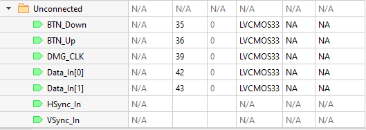
Good evening, I'm having some issues with some verilog code, or quiet a lot to be honest. Or with Lattice's software actually.. This was tried in Lattice Radiant. First off, I'm getting these warnings(I know they're called 'error' I moved their severity up to make them stand out more). The other 106 errors are related to the .ldc file statements and some severity list statements missing
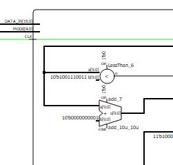
but when viewing the netlist analyzer they all seem to be connected.

In the Device Constraint Editor they'll show up as unconnected and I cant assign any pin locations to VSync_In and HSync_In.
 It's programmed in lattice Radiant, with atom as the text editor, the selected FPGA is the UP5k-SG48(ice40 board) and the verilog version is 2001. I tried; adding the complete pin declaration in the module definition, removing the 'wire' statements, going with different names and more things I can't remember anymore. But alas, nothing worked so far. I included a trimmed version of the code below, I removed all block which aren't related to the pins or only after another module.
// Made by yours truly with the intention of learning Verilog and VHDL
// The idea is to convert the DMG video output to VGA and optionally even CGB video.
module DMGtoVGA(
    // MCLK,
    RST,
    EN,
    BTN_Down,
    BTN_Up,
    HSync_In,
    DMG_CLK,
    VSync_In,
    Data_In,
    Vsync_Out,
    Hsync_Out,
    B,
    G,
    R,
    spi_ssn
);

/*  SPI-Flash pinout  */
// output wire spi_sck;       //SPI Slave ClocK
output wire spi_ssn;       //SPI Slave Select Negated
// inout wire spi_cs;         //SPI Chip Select ~duplicate of spi_ssn
// output wire spi_mosi;      //SPI Master out, Slave in
// input wire spi_miso;       //SPI Master in, Slave out
assign spi_ssn = 1'b1 ;                   // Disable SPI Flash after configuration

// input wire   MCLK;
input wire RST;
input wire BTN_Down;
input wire BTN_Up;
input wire EN;
input wire HSync_In;
input wire DMG_CLK;
input wire VSync_In;
input wire [1:0] Data_In;
output wire Vsync_Out;
output wire Hsync_Out;
output wire [3:0] B;
output wire [3:0] G;
output wire [3:0] R;

wire    Frame_Sync;
wire    VGA_CLK;     //40MHz VGA pixel clock
wire    CLK_HF;      //internal oscillator output(48MHz)
wire    CLK3DIV;     //Custom devision of the internal HF oscillator
wire    [0:4]PSMode; //pallete selection control input


//Button debouncing
wire Deb_Up, Deb_Down;
FILTER
Up_deb1 (
  .FILTERIN  (BTN_Up),  // I
  .FILTEROUT (Deb_Up)   // O
);
FILTER
Down_deb1 (
  .FILTERIN  (BTN_Down),  // I
  .FILTEROUT (Deb_Down)   // O
);


//Pallete selection
PalleteSelector PS_inst(
    .Up(Deb_Up),
    .Down(Deb_Down),
    .Err(1'b0),
    .MODE(PSMode)
    );

    wire [15:0]DMG_PixelData;
    wire [15:0]VGA_PixelData;
    wire [13:0]VGA_PixelADDR;
    wire [13:0]DMG_PixelADDR;
    wire RAMRDWR_1;
//Decode the DMG input to synced Pixel_Data, any custom pallettes are applied here
DMG_Decoder DMG1_inst(
    .CLK(CLK3DIV), //MCLK
    .RST_n(RST),
    .EN(EN),
    .VSync(VSync_In),
    .Hsync(HSync_In),
    .DMG_CLK(DMG_CLK),
    .Data_In(Data_In),
    .Sync(Frame_Sync),
    .Wren(RAMRDWR_1),
    .Data_Out(DMG_PixelData),
    .Ram_Addr(DMG_PixelADDR)
    );

//PSRAM buffer between VGA and input, should be big enough even for the CGB ':)
//for now only 1x 256Kb bank(32KB is needed)

SP256K SPRAM_inst1 (
  .AD       ((RAMRDWR_1) ? DMG_PixelADDR : VGA_PixelADDR),  // I
  .DI       (DMG_PixelData),  // I
  .MASKWE   (4'b1111),  // I
  .WE       (RAMRDWR_1),  // I
  .CS       (1'b1),  // I
  .CK       (CLK3DIV),  // I
  .STDBY    (1'b0),  // I
  .SLEEP    (1'b0),  // I
  .PWROFF_N (RST),  // I
  .DO       (VGA_PixelData)   // O
);

endmodule
Lol, and this isn't even everything. Apparently, the SPRAM module doesn't want to be initialized. But that can wait, I've been at this for a whole week now and it's getting annoying.


HSync_In!=Hsync_In. The synthesis errors use the latter, but your code seems to be the former. \$\endgroup\$