0
\$\begingroup\$

I built an open-loop-controlled buck converter in Simplis. The parameters are listed below:

\$V_g=12V,V_{out}=5V\$

\$D=0.52\$

\$C=100\mu F,ESR=5m\Omega; L=30\mu H,ESR=5m\Omega\$

I use Simplis to simulate the bode plot of \$G_{v_d}\$. And I use the Mathcad to simulate the same circuit. But the result was different. During the low frequency, the peak gain margin in Simplis is less than 0db, while in the Mathcad, the gain was about 20DB.

Here are the results I got.

the circuit in Simplis

the circuit in Simplis the Gain bode plot in Simplis

the Gain bode plot in Simplis

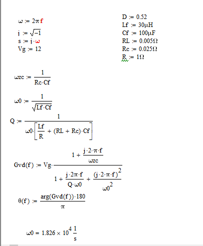
the code in Mathcad

the code in Mathcad

the curve in Mathcad

the curve in Mathcad

I don't know what kind of mistake leads to this result. If someone knows the reason, would you please tell me? I am a freshman in Power electric and I appreciate your guidance .

\$\endgroup\$
6
  • \$\begingroup\$ What about Ron for the FET & diode? Not 0? \$\endgroup\$
    – D.A.S.
    Commented Mar 9, 2021 at 4:25
  • \$\begingroup\$ Also V5 must be >2* Vgs(th) max =>8V pref 2.5 x unless you were given to use this in app. \$\endgroup\$
    – D.A.S.
    Commented Mar 9, 2021 at 4:32
  • \$\begingroup\$ ESR for cap = 5mOhm ? or 25mOhm which sounds more reasonable. If Ron =0 Q= 25 dB \$\endgroup\$
    – D.A.S.
    Commented Mar 9, 2021 at 4:39
  • \$\begingroup\$ Very underdamped even with 5m switch tinyurl.com/y7puk4yt \$\endgroup\$
    – D.A.S.
    Commented Mar 9, 2021 at 5:04
  • \$\begingroup\$ Thanks so much, I haven't considered these things in detail. I need to research more about them definitely. There are still lots of unknown things to me. \$\endgroup\$
    – Linda Yu
    Commented Mar 9, 2021 at 8:19

2 Answers 2

1
\$\begingroup\$

The control-to-outout transfer function of the CCM buck operated in voltage-mode control is the following:

enter image description here

Several comments regarding your results:

  • in Mathcad, you have missed the pulse-width modulator (PWM) gain which is \$G_{PWM}=\frac{1}{V_p}\$ with \$V_p\$ the peak of the modulation ramp. This is your source \$V_3\$ in the SIMPLIS file. It must obviously appear in the control-to-output transfer function that will use for analytical results.
  • the quality factor includes many contributors as you can see. In the formulas, these are values of passive elements such as ohmic losses of the capacitor and inductor. In reality, other losses affect \$Q\$ such as the MOSFET \$r_{DS(on)}\$, the diode recovery losses and even magnetic losses. This is the reason why you may see differences between your Mathcad analysis and the SIMPLIS one or a bench prototype. To make sure you have very close results between simulations and Mathcad, chose perfect switches in SIMPLIS (and not a MOSFET), 0-\$V_f\$ diodes etc. Finally, you may be interested to import SIMPLIS simulation results directly in Mathcad to superimpose magnitude and phase curves. See here for a tutorial.

Finally, you can have a look at the 60+ simulation templates I posted here for my next book on small-signal modeling of switching converters (TOC is here). Most of the examples work on Elements, the demo version and you can explore many structures.

\$\endgroup\$
12
  • \$\begingroup\$ Thanks so much, I realized the problem might occur because of the transfer function, but I didn't know how to derive it. Your answer is instructive. The resource you provided is also helpful, I will research it further. \$\endgroup\$
    – Linda Yu
    Commented Mar 9, 2021 at 8:02
  • \$\begingroup\$ This is good, I'm glad if I can help. Please acknowledge the answer if this what you were looking for, thank you. If you are interested in small-signal modeling, you can have a look at my APEC 2013 and APEC 2014 seminars or more specifically on the buck with APEC 2019. \$\endgroup\$ Commented Mar 9, 2021 at 9:55
  • \$\begingroup\$ excellent answer. Reminds me of my time with Keith Billings in the 80's qualifying his designs \$\endgroup\$
    – D.A.S.
    Commented Mar 9, 2021 at 10:20
  • \$\begingroup\$ Merci Monsieur Stewart, I have been in touch several times with Keith long time ago : ) \$\endgroup\$ Commented Mar 9, 2021 at 10:21
  • \$\begingroup\$ Mei oui. He wrote the 1st book. Brown was another expert. \$\endgroup\$
    – D.A.S.
    Commented Mar 9, 2021 at 10:29
1
\$\begingroup\$

Additional info and important take-aways on ideal lossless open-loop Buck converters: ( THINGS can go horribly wrong with the wrong load)

The equation for Q for \$r_C=r_L=r_{SW}=0,~~~\$, \$Q=C\omega_o,~~~~ Q=C\sqrt{\dfrac{1}{LC}} =R_L\sqrt {\dfrac{C}{L}}~~~~~~~~, \$ \$\omega_o=\dfrac{1}{2\pi f_o}\$

This only works when the SMPS is loaded. Otherwise with no load Q rises to infinity with RL.

So for the critical damping load = \$Q=1/2\zeta_{(zeta_=0.707)}~~~= C\sqrt{\dfrac{1}{LC}} =R_L\sqrt {\dfrac{C}{L}}\$

  • thus the critical value is \$R_L=\sqrt{\dfrac{L}{8C}}\$
    • If R is 10 times higher it will look like below. enter image description here

Then for Vpp ripple voltage to be <=1% f must exceed the value for dV/dt=Ic/C where \$dt~ 1/2f\$ so \$f_{min}=\dfrac{Ic}{2C*dV}\$ for Vpp=dV

I'll let you figure out f(min) for Load=1.5A, L=100uH, C=100uF, R=3.3 and dV=dI*R 0.1% of Vout=5V = 5mV, assuming ideal rC=rL=rSW=0. but Ic is not load current.

(this is why IC's use more complex startup Imax, good stability and ripple compensation)

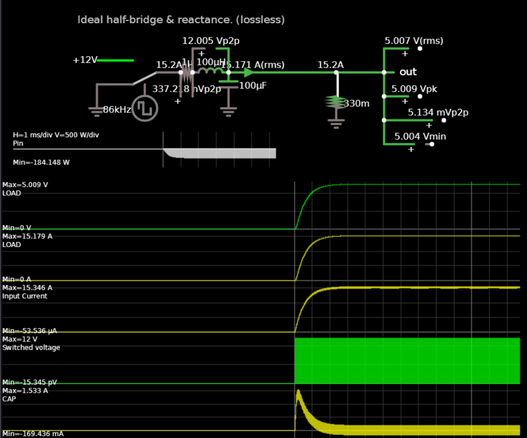
Here again ideal Open-Loop but with a critical damping load.

enter image description here

Interactive Browser Simulation by Falstad

\$\endgroup\$
1
  • \$\begingroup\$ thanks so much, so changing the load could result in the damping factor Q of the transfer function. I will derive it by myself later. The simulation is really intuitive. \$\endgroup\$
    – Linda Yu
    Commented Mar 11, 2021 at 3:35

Your Answer

By clicking “Post Your Answer”, you agree to our terms of service and acknowledge you have read our privacy policy.

Not the answer you're looking for? Browse other questions tagged or ask your own question.