1
\$\begingroup\$

Recently I began a project involving some active current limiting using a MOSFET and an Op Amp. It is part of a larger overall circuit involving other Amplifiers.

I would like to perform a block-diagram-style analysis on my circuit in order to investigate loop gain and stability. However, I was stuck when it came time for me to analyze the MOSFET's transconductance behavior. The simplified example below illustrates my problem: enter image description here
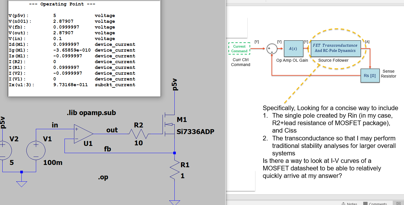
The circled block in the above diagram is what I'm trying to unpack. As stated in the diagram, since this is part of a stability analysis, I really only need the RC pole location and the transconductance.

Is there a way to model any MOSFET Trans conductance amplifier as a single-pole Transfer Function?

Furthermore:

How would I go about extracting the necessary parameters from I-V curves within the MOSFET datasheet?

EDIT: More details on what I'm looking for: I understand my dummy example has stability concerns due to the OA's dominant pole and the additional pole from the series R and the MOSFET's Ciss. Of course this leads to instability in some scenarios.

I want to know how to pull out the MOSFET's behavior into its own "block" as seen in the block diagram in my post. I assume its "block" looks something like gm*{Something}/(1+s{Some_Tau}). I'm wondering how to extract the "something" and "some_tau" from datasheets within some reasonable tolerance. I know Ciss varies somewhat, but I'm fine with some reasonable accuracy.

\$\endgroup\$
1
  • \$\begingroup\$ Could be one or two poles, depending on the capacitances and gains. Look up some of the better online academic class notes for the "miller approximation" and it will review this. first google hit ... The Zout of the op-amp would have to factor in too, I suppose. \$\endgroup\$
    – Pete W
    Commented Mar 10, 2021 at 3:55

2 Answers 2

1
\$\begingroup\$

If you want to model it choose the exact part and simulate it , otherwise Ciss increases with decreasing gate R and RdsOn both dynamically during conduction and with bigger parts. So a 1st order model is Rs + Rg+ Ciss, I believe.

However Zo on Op Amp’s rise to the R equivalent or current limit for sub microsecond slew rates e.g. 220 Ohms for BJT types which lowers the pole.

it depends on your acceptable voltage error, slew rates and loop response time required and step load regulation error. Obviously worse for switched reactive loads. So as others have said phase lead compensation helps. .. With RC +R feedback. Simulate it if not sure then breadboard it under dynamic disturbances like a step load.

\$\endgroup\$
2
  • \$\begingroup\$ I should have clarified, I understand about the stability concerns here. I know the OA has its dominant pole, and the MOSFET introduces another pole. What I really want to know is how I can treat the MOSFET as its own "block" in the block diagram shown in my OP. I assume it has the form gm*{something}/(1+sTau), but I'm not sure how to identify the missing terms. \$\endgroup\$ Commented Mar 10, 2021 at 2:22
  • \$\begingroup\$ en.wikipedia.org/wiki/Common_drain & en.wikipedia.org/wiki/Common_source \$\endgroup\$
    – D.A.S.
    Commented Mar 10, 2021 at 3:48
1
\$\begingroup\$

Is there a way to model any MOSFET Trans conductance amplifier as a single-pole Transfer Function?

In this circuit the FET gate is driven from the opamp's output. If the opamp has the usual single pole compensation, then it has a low frequency pole. Then the opamp's output impedance and gate resistor introduce a second pole together with the FET gate capacitance. This usually makes this circuit unstable, so you need an extra compensation capacitor. If the opamp's output impedance varies with frequency, YMMV.

FET capacitance varies a lot with Vgs, moving the frequency of the second pole around.

FET transconductance varies with Id, which changes the gain.

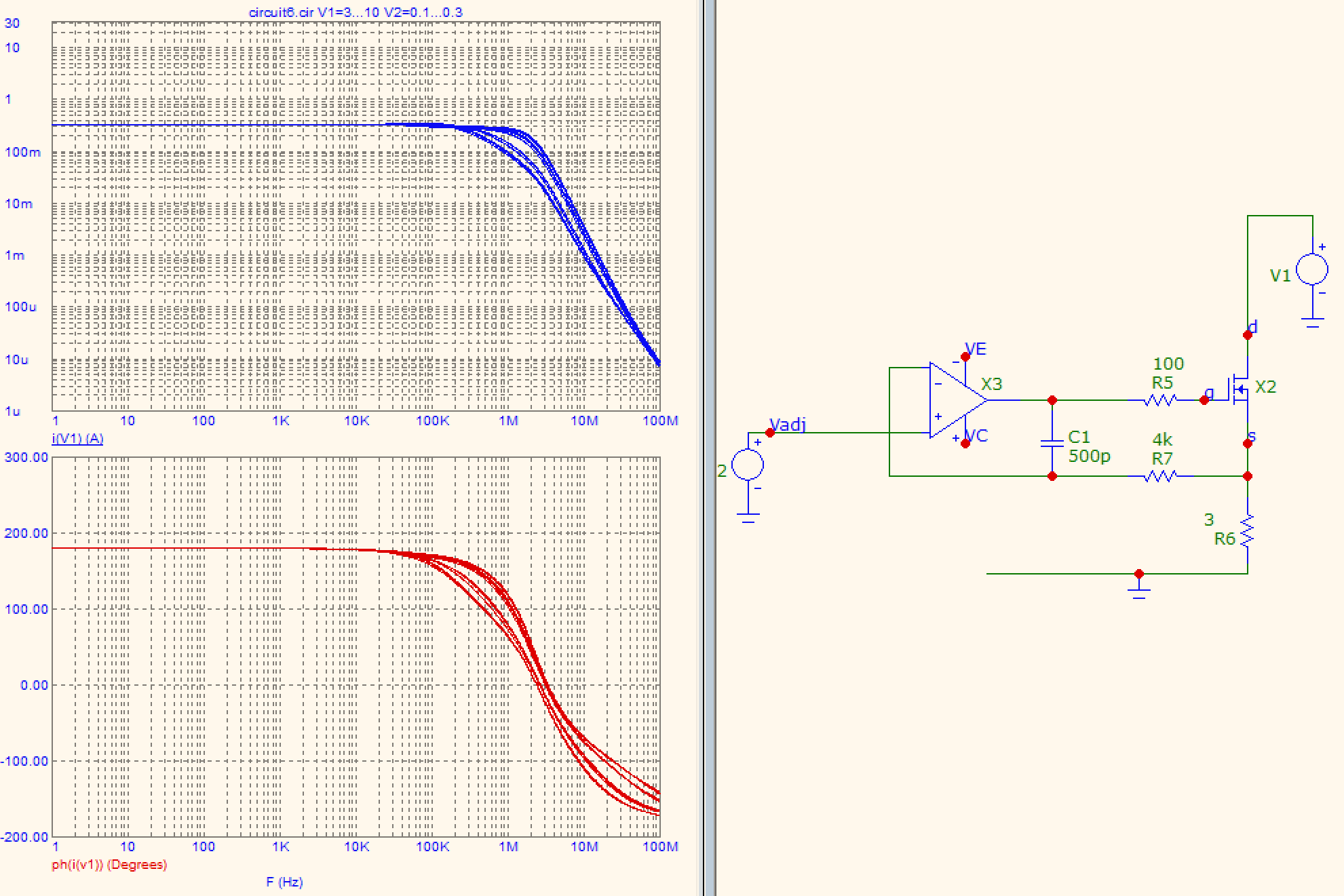
This is the closed loop response with AC stimulus on input "Vadj", and stepping DC values on both Vadj and V1 (output voltage).

enter image description here

The closed loop transconductance response has two poles and moves around quite a bit depending on current and output voltage.

EDIT:

What I really want to know is how I can treat the MOSFET as its own "block" in the block diagram shown in my OP. I assume it has the form gm*{something}/(1+sTau)

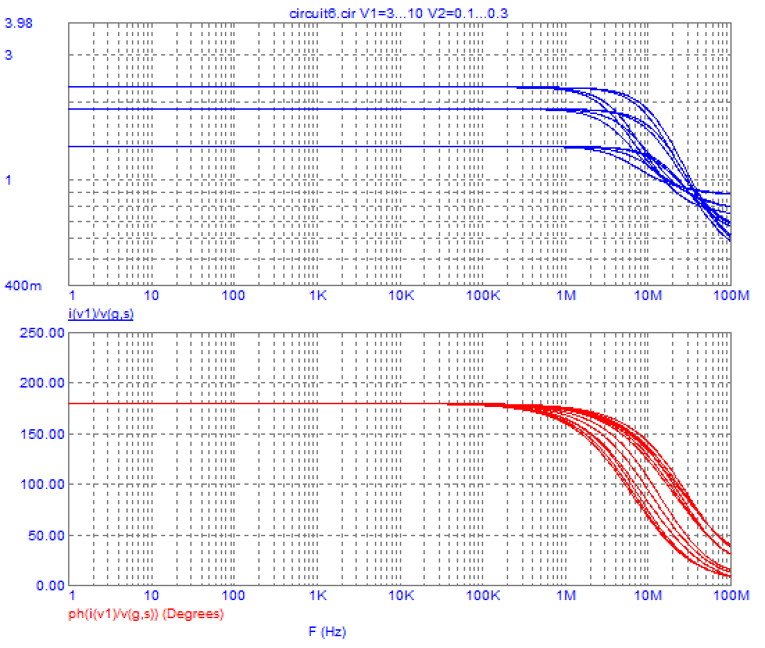
Not really. Plotting the transconductance of the FET (Iout/Vgs) and its phase:

enter image description here

In a common source, you get 2 poles there. Let's choose a positive polarity for the output current (ie, positive when the FET sinks current), that's easier to visualize.

When gate voltage increases and the FET is in control, output current also increases. More Vgs, more sink current, positive transconductance.

But when frequency is high enough that the FET is no longer in control, because its capacitances dominate the opamp's output drive capability, you can replace the FET with a pair of capacitors, Cgs and Cgd. Some of the gate drive signal passes through Cgd and directly into the output, and this creates a current that is of opposite polarity of what the FET drain current would be.

So, when gate voltage goes up, through Cgd output voltage tries to go UP, which means sink current goes down... So, 180° phase shift, two poles.

\$\endgroup\$
5
  • \$\begingroup\$ I should have clarified, I understand about the stability concerns here. I know the OA has its dominant pole, and the MOSFET introduces another pole. What I really want to know is how I can treat the MOSFET as its own "block" in the block diagram shown in my OP. I assume it has the form gm*{something}/(1+sTau), but I'm not sure how to identify the missing terms. \$\endgroup\$ Commented Mar 10, 2021 at 2:19
  • \$\begingroup\$ Got it. So seems like my MOSFET "block" will be a slightly more complicated mess. I suppose I'll just find my gm from my operating point, and do some small-signal modeling to get appropriate equations. I'll edit my post with my solution when I get around to it. \$\endgroup\$ Commented Mar 10, 2021 at 13:04
  • \$\begingroup\$ You could try to use the ready to find documentation about small signal MOSFETs, but those parameters will involve calculations that depend on the dynamical usage of the circuit: you have a feedback that settles at a certain operating point (assuming static operation). In the end, this method might be easier since it's a one click away (plus cursors or .meas statements). Otherwise, here's a quick hack for a MOSFET (not VDMOS, what you have there), that shows an equivalent circuit that might be used with a bit of tweaking. \$\endgroup\$ Commented Mar 10, 2021 at 13:15
  • \$\begingroup\$ Here's another thing. The opamp has a pole so it needs a compensation cap which is set for the worst case (low Vds). But at high Vds the FET performs much better than worst case, so a lot of open loop gain is wasted through the compensation cap instead of being used to improve the performance of the circuit. If the FET gate is driven not with voltage, but with current instead, the variable capacitance (depending on Vds) results in variable gain, and the lower capacitance/higher gain at higher Vds can be used instead of wasted. \$\endgroup\$
    – bobflux
    Commented Mar 10, 2021 at 13:19
  • \$\begingroup\$ This scheme makes the FET capacitance the dominant pole. But then, to drive it with current you need a transconductance amp. If you don't need DC accuracy, a single bipolar transistor will do the job very well as a transconductance amp. But if you need DC accuracy, it's more complicated. So it depends what the goal of the whole circuit is. \$\endgroup\$
    – bobflux
    Commented Mar 10, 2021 at 13:20

Your Answer

By clicking “Post Your Answer”, you agree to our terms of service and acknowledge you have read our privacy policy.

Not the answer you're looking for? Browse other questions tagged or ask your own question.