0
\$\begingroup\$

enter image description here

Sorry I mixed up the two diagrams, I thought both diagrams were using FETs on the right side.

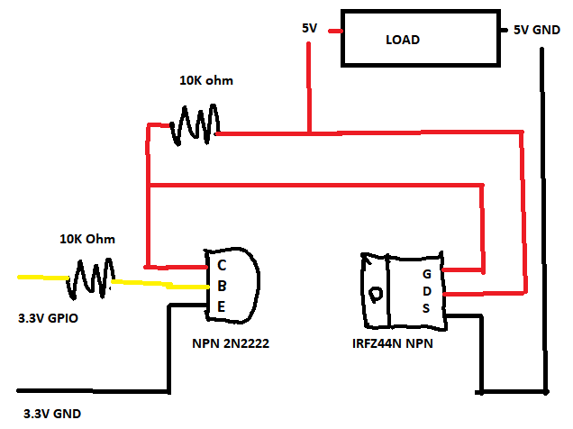
I am trying to turn on a 5V separate power source with a 3.3V GPIO output. I have two separate circuits, the 3.3V one is a deep sleep ESP-01 that's turning on a bigger microcontroller with its own battery/bunch of sensors. So I'm doing the NPN to PNP switch approach. I found the diagram on the right after someone suggested I use a high-side switch approach(I was using low side before and I was having weird power problems). I also have IRF9640PBF MOSFETs if those are better.

As mentioned I don't understand how you put a load on a seemingly positively wire (right image below +12V). I'm assuming the LOAD would be my second circuit/larger microcontroller.

Thanks for any help

edit: I have the wrong diagram on the right, I updated it. I'm updating my MS paint circuit.

Going to try this, matches left-most diagram enter image description here
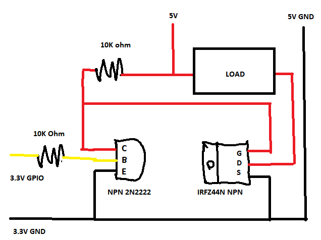
That's not good, the step down converter started squealing haha. You are failing doctor...

enter image description here

Well I gotta go through this some more, figure out what's going on.

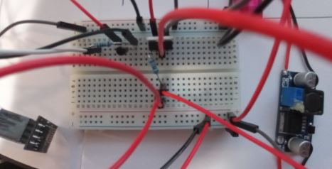
This one the step down regulator is happy, however I can't tell if my electronic switch is not working or it's just literally not connected (MOSFET source). The IRZ44N needs a 4V gate threshold not sure if that's why, will try it with my power supply. I'll respond to this when I figure it out, seems like I gotta go back to the basics.

enter image description here

\$\endgroup\$
7
  • 1
    \$\begingroup\$ I can tell there's some kind of major disconnect in understanding here--you don't put a load "on a wire", positive or negative--you put a load between a positive and negative (or live and neutral). But I'm too sleepy to figure out how to explain it right now. \$\endgroup\$
    – Hearth
    Commented Apr 3, 2021 at 2:54
  • 1
    \$\begingroup\$ Swap the drain and source on your PMOS (which you have labelled as a PNP but is not a PNP). Then swap your Load and PMOS. And in your schematic that has a PNP, it will fry if you pull it LO with the NMOS because no resistor is there to limit current. If it is a PMOSs it will be fine without a resistor. \$\endgroup\$
    – DKNguyen
    Commented Apr 3, 2021 at 2:55
  • \$\begingroup\$ Yeah I messed this up, I thought both diagrams were using PNP fet or transistors... I gotta fix this. \$\endgroup\$ Commented Apr 3, 2021 at 2:58
  • \$\begingroup\$ PNP or NPN refer to bipolar transistors. MOSFETs are either PMOS or NMOS. \$\endgroup\$ Commented Apr 3, 2021 at 3:23
  • \$\begingroup\$ Oh... that's good to know crap. I think I thought of it that way because of "P-N channel" I got it, but I see it from the P/NMOS. I still don't understand what load means... a resistor is a load/can go in line with "positive"... I guess I would just tap into the load with a connection to GND to power my larger circuit? \$\endgroup\$ Commented Apr 3, 2021 at 3:25

2 Answers 2

1
\$\begingroup\$

A circuit requires a closed loop to operate. Therefore one could either disconnect the V+ or 0V line to the load and no current will flow through the load.

Transistor switching circuits come in two varieties.

  1. "High Side Switch" , sits between v+ and load and disconnects V+

  2. "Low Side switch" sits between load and 0V and disconnects 0V

You have a low side switch schematic, but there are also some other errors associated with it, so it is not so important to illustrate the concept.

From a purely electrical perspective and a basic load they are equivalent, for example, if your load is a heater coil or light bulb then it doesn't matter which side you switch.

There are secondary effects, in complex circuits there may be many things referenced to 0V, it could be considered a safety hazard to have the load energized to V+ . For example if the load is a heater coil, using a low side switch will leave the coil at V+ potential, a grounded technician with reference to 0V is therefore at risk electric shock when the switch is off.

\$\endgroup\$
1
  • \$\begingroup\$ Both of the legit diagrams on the right are low side? I thought they were high side. Is it a high-side switch if the load is on the GND side? \$\endgroup\$ Commented Apr 3, 2021 at 3:09
1
\$\begingroup\$

Generally speaking, there are two ways in a DC circuit to switch power to a load with transistors:

  1. Connect one side of the load to GND, and switch the other side up to a positive DC voltage.

  2. Connect one side of the load to a positive DC voltage, and switch the other side to GND.

The schematic on the right is a not-quite-correct example of method #1. It is missing a base current limiting resistor between the Q? collector and the Q? base.

The schematic on the left looks like an attempt at method #2, but for that you need a logic-level n-channel MOSFET. If you can adjust the output signal logic polarity in firmware, you can eliminate the 2N2222 and its base resistor

NOTE - this type of discussion is MUCH easier with correct reference designators.

NOTE: The left-side schematic just changed. Now, the MOSFET places a dead short across the 5 V power supply.

\$\endgroup\$
5
  • \$\begingroup\$ Yeah sorry this is not my field at all(coming from software). I know people said to use Kicad/not MS Paint. The issue is I need to turn the large circuit on by a high GPIO out. So that when the smaller circuit is off, the larger circuit is also off. I will adjust my attempt with an NPN MOSFET hopefully the ones I have will work. I have IRL7833 and IRFZ44N not sure which one is better, the former is logic-level. I think the high-side thing on it's on (single FET) before I switched to transistor-transistor would pull down low (GPIO LOW). But I went to tx to tx due to 3.3 to 5V \$\endgroup\$ Commented Apr 3, 2021 at 3:07
  • \$\begingroup\$ I wonder if the dead short you mentioned is why my step down converter starts making a sound that gets louder. I have to go through this again. \$\endgroup\$ Commented Apr 3, 2021 at 5:44
  • \$\begingroup\$ I got it wired where it doesn't have the short now, will update diagram, hopefully this works. I can't tell if the left pro diagram is using a pull up or down switch (3v3 GPIO) will try both. Although one problem I seem to have with this config is my ESP-01 won't boot if GPIO2 is connected to the circuit. \$\endgroup\$ Commented Apr 3, 2021 at 6:00
  • \$\begingroup\$ GPIO2 is used to put the esp8266 into bootloader mode. Use another GPIO or get a module with more GPIO. The IRFZ44 is not the best choice for running at 5V. \$\endgroup\$
    – Kartman
    Commented Apr 3, 2021 at 7:58
  • \$\begingroup\$ Thanks for the thoughts... I'm stuck with this currently. I think I literally have to learn the basics of how transistor/mosfet works to do this. I'd like to just pay someone to give me a circuit that'll work with my parts ha but that's a pain in and of itself. Anyway I may be using GPIO0 I have used this setup before and it worked fine... perhaps something with this particular circuit is bad that stops the boot from working. \$\endgroup\$ Commented Apr 4, 2021 at 9:47

Your Answer

By clicking “Post Your Answer”, you agree to our terms of service and acknowledge you have read our privacy policy.

Not the answer you're looking for? Browse other questions tagged or ask your own question.