0
\$\begingroup\$

I need to solder a tiny 3 mm by 5 mm SMD. Thankfully my school has a reflow oven that can do the actual soldering part, but I still need to accurately get the solder paste on there, so I was thinking of making a stencil.

We also have a laser cutting machine but it can't cut through metal and using other things like plastic results in the "threads" between the pads being so thin that they break. (BTW is there another material like Kapton film that could be cut super think and not break?)

Is there a way to manipulate a Gerber file so that a PCB machine will cut out holes straight through the area where the pads should be?

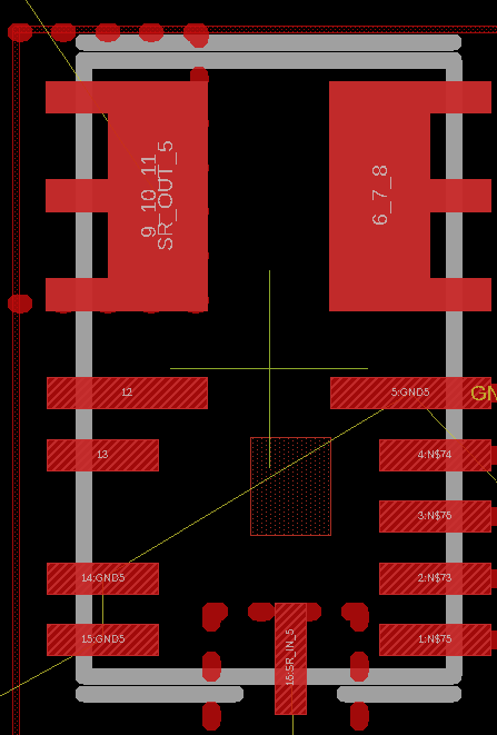
enter image description here

For example, using the picture for reference, create a Gerber file that tells the PCB machine to cut holes where the red pads are in the picture (not the red dots).

\$\endgroup\$
6
  • 3
    \$\begingroup\$ Your layout program can probably output a stencil layer as a Gerber \$\endgroup\$ Commented Apr 9, 2021 at 1:07
  • 2
    \$\begingroup\$ You can dispense the paste manually with a syringe. You don't need a stencil unless you are going to make a lot of boards. mouser.com/productdetail/chip-quik/… \$\endgroup\$
    – user57037
    Commented Apr 9, 2021 at 2:14
  • \$\begingroup\$ mouser.com/ProductDetail/Chip-Quik/… \$\endgroup\$
    – user57037
    Commented Apr 9, 2021 at 2:14
  • \$\begingroup\$ But to answer your question, PCB layout tools can generate stencil layers (and usually do). The solder mask layer from the gerbers will be very similar to the stencil artwork. If you only have access to gerbers, you can probably start with the solder mask layer and use a gerber tool to make stencil artwork. The stencils themselves are usually laser cut from stainless steel sheet that is around 0.1 to 0.15mm thick. Once you have stencil gerbers you can just send them to a PCB fabricator for a quotation. The stencil will have to lay flat on the board. There can't be any obstructions. \$\endgroup\$
    – user57037
    Commented Apr 9, 2021 at 2:22
  • \$\begingroup\$ If you have to manipulate the gerbers, it may be worth buying viewmate deluxe from pentalogix. (A gerber tool). \$\endgroup\$
    – user57037
    Commented Apr 9, 2021 at 2:23

3 Answers 3

1
\$\begingroup\$

I'm going to use Elegoo 3D printer for my stencils.

It's extremely precise and the resolution is 0.05 mm in x, y and z.

\$\endgroup\$
1
  • \$\begingroup\$ Interested to see a follow up. You can print locating features. \$\endgroup\$ Commented Apr 9, 2021 at 7:10
0
\$\begingroup\$

We use to make folded tin-plated brass EMI shields etched from a local PCB shop and made the etch double sided so holes were on both sides and folds on 1 side so it etched only half way thru. Any shop that can do 10 mil track and gap etching ought to be able to make a small panels worth with a setup cost. Pads may need a butterfly shape for better deposits of paste. I don’t recall the details. We also made artwork files to be printed to film from lithographic printers for $50 30 yrs ago then etch them in house with heat and agitation flow of acid. There are also local,laser printing shops in Toronto with very sharp <0.1mil features flow thru acid etch that may be cheaper than the screen printer shops (IDK) and they give really high resolution and clean edges.

Better to go shopping for SS laser cut or forced acid etch screens. I might still have a card laying around that looks like a Remington steel electric screen business card with Art Deco.

\$\endgroup\$
0
\$\begingroup\$

The most ghetto stencils I’ve seen were where on a YT video where the guy straightened out aluminum from soft drink cans and etched it using the old toner transfer method.

I can't recommend it directly, I've only used framed laser-cut stainless stencils, but it looks feasible for those with time and access to the etchant chemicals.

Polyester (Mylar) is an alternative to polyimide (Kapton) but if the laser won't cut the Kapton the way you want it, I suspect polyester won't be much better.

If you glued down thin metal to some kind of a sacrificial substrate it's possible that a PCB milling machine would handle it, then you'd need to release the stencil material, perhaps by heat, after removing the burrs on the top with some light sanding. Kapton adhesive tape might be usable directly for a one-time stencil (just stick it to blank substrate and mill it).

But I bet you could get that one part to solder okay by tinning the part and the board lightly (remove excess with a braid), clean off both sides in isopropanol then slather both parts with copious amounts of liquid flux, and run it through the reflow just to get that part soldered.

\$\endgroup\$

Your Answer

By clicking “Post Your Answer”, you agree to our terms of service and acknowledge you have read our privacy policy.

Not the answer you're looking for? Browse other questions tagged or ask your own question.