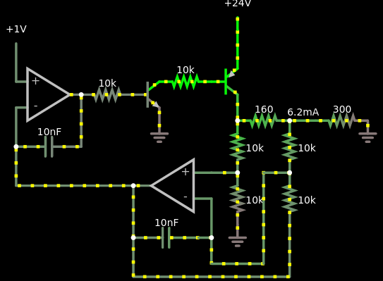
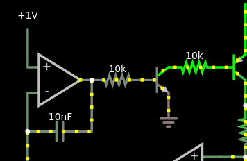
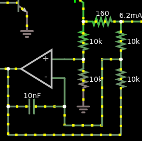
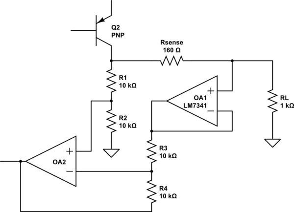
... in practice, the output varies depending on the load of 300 ohm resistor. If I using a 1k ohm resistor, then I get a different output current.
This means that, for some reason, your circuit does not fulfill its main purpose of maintaining a constant current.
Conceptually, the circuit solution is correct. Because the load is grounded, the current is measured through a high side "floating" current-sensing resistor... and this requires the use of a differential amplifier.
The two transistors form not exactly a Sziklai pair because the emitter of the NPN transistor and the collector of the PNP transistor are separated... but this is not so important here.
The problem here, in my opinion, is that the PNP transistor cannot be reliably cut off when the NPN transistor is cut off (I have explained why here). This problem can be solved by connecting a (few k) resistor between its base and emitter and adding a "shifting" Zener diode in series to the base resistor.
Also, the PNP transistor should be always in active mode (with some voltage drop VCE > 1 V). Search in Google with "current source compliance voltage".
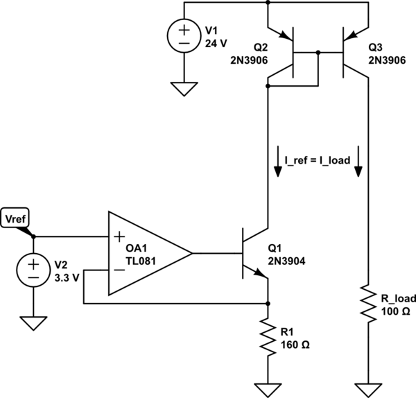
EDIT: I would like to consider the Dave's circuit solution (through a current mirror) by comparing it with the OP's solution. At first glance, they are completely different, but I will try to convince you that, in a sense, they are the same.
Both solve the same topological problem - they reverse the direction of the collector current of the NPN transistor. In the OP solution, the humble PNP transistor does this because its collector current has the opposite direction to the base current. In the Dave's classic current mirror, the PNP Q3 does this. So, in regards to the current direction, both they act as *current inverters"... both they are current mirrors...
In regards to the current magnitude, the OP's "1-transistor current mirror" (like every BJT) is an amplifier (Ic = beta.Ib) while the Dave's classic current mirror is a follower. It is interesting to see how this current ampifier is made act as a follower since unraveling this mystery would be a possible scenario for the current mirror inventing (very important for understanding).
The trick is simple - the excessive base current is diverted by an additional element connected in parallel to the PNP base-emitter junction (current divider). In the simple case, it can be a resistor (as I suggested above). Only, the resistor is linear while the base-emitter junction is non-linear and its resistance should be carefully adjusted (still it is used in MOSFET current mirrors).
A diode can serve as a good diverting element since actually the base-emitter junction is a "diode"... but they are not exactly the same. The perfect diverting element is a transistor made act as a diode - the so-called "active diode" (Q2).
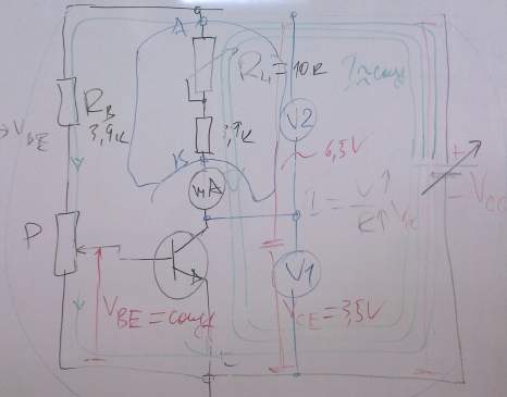
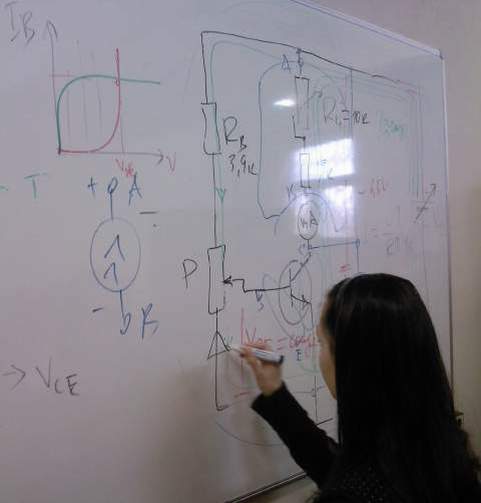
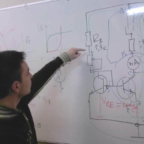
On April 8, 2008, I conducted three consecutive labs dedicated to this kind of transistor current sources. After that, I wrote, with the help of my students, three
exciting Wikibooks stories about how they and I "invented" the famous current mirror circuit:

Fig. 1. Building the simplest transistor current source

Fig. 2. Trying to create a diode current mirror

Fig. 3. "Inventing a BJT current mirror
To write them, I recorded these "lab brainstorming sessions" on a solid-state recorder and made photos in the lab.
As a conclusion
Basically, both circuits do the same - they measure the load current by measuring the voltage drop across a stable (160 ohm) current-sensing resistor. The difference is that the OP's "amplifying current mirror" is inside the negative feedback loop while the Dave's true current mirror is outside the loop. So the former can be imperfect while the latter must be perfect. From this point of view, one can reach the paradoxical conclusion that, in a sense, the OP circuit is better:)
The problem of the simple BJT mirror is that it is based on the passive compensation (without negative feedback). But the simple op-amp differential amplifier is also based on this passive principle and it requires precise matching the four resistors.

