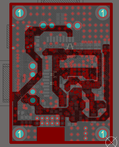
I'm working on a Raspberry Compute Module 4 Carrier with an USB 3.0 Controller with High Speed signals. As I read here in other thread, I decided change polygons for power planes, but I have 2 doubts about them:
-What can I do with the white space? I have 4 split planes, Should I connect all the excess plane to GND or one of the power supplies?
-Other doubt, Can I route high speed signals over power split planes? I have read about not routing over ground split planes, but I'm not sure if I can do with power planes.
About differential pair impedance, the height of the trace is from their respective planes or from GND plane? I'm not sure from where I should to measure the height (my stack up have 4 layers).
Thank you so much!
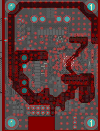
Edit: Thank you so much for your answers. I have reorganized the PCB and avoid that the traces cross split planes. On Texas Instruments Forums I have received an answer that recommends to me doesn't route on power planes references, he advice to me change my design to 6 layers. Other mate here have told to me that route my signals in inner layers but Texas Instruments doesn't recommend route high speed signals on inner layers. Is the best option add more layers?


