3
\$\begingroup\$

I am using a DMP3007 as a reverse polarity and over voltage MOSFET. The maximum planned load is 10 A and voltage may vary as the load is a constant current load.
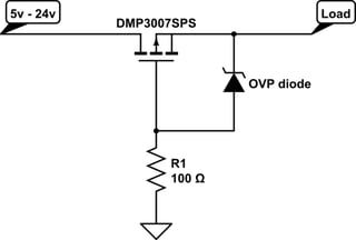
schematic

simulate this circuit – Schematic created using CircuitLab

When in this configuration does the MOSFET conducts at its lowest resistance? Assuming it does the power consumed with respect to the value given by the datasheet would be:

P = RII

P = 0.007 ohms * 10A * 10A

P = 0.7 watts

0.7 watts is lower than the rated total power dissipation of 1.4 W, so am I correct that I wont be needing a heat sink?

lets assume that I will raise the load to 15 A instead of 10 A, this means that the power consumed will be 1.575 W which is greater than 1.4 W. Instead of placing a heatsink can I dissipate the extra 0.175 W into the PCB? To do that I need to beef up the PCB trace/fill of which pin? I assume its the drain pin because it the largest pin? How much copper area do I need to have to dissipate that 0.175 W? Assuming 1 oz copper thickness

\$\endgroup\$
16
  • 7
    \$\begingroup\$ NO NO NO That "0.007 ohms" is when the MOSFET is FULLY SATURATED (fully on). $$$$ In this circuit, you are not guaranteed it will always be fully on! The diode is not a hard switch... There is going to be a significant region where it's just starting to turn on, which will just barely start to turn on the MOSFET. At this point, the MOSFET has a MUCH higher resistance than 0.007 ohms. When fully on, your calc is right. But you can't know you'll always be operating there. Especially with a 5:1 possible input voltage range. $$$$ I think you need a more sophisticated circuit \$\endgroup\$
    – Kyle B
    Commented Jun 7, 2021 at 15:55
  • 3
    \$\begingroup\$ Not quite.. The MOSFET will pass through ALL resistances from infinity (not on, open circuit) to effectively a short circuit (0.007 ohms). All transistors work this way, you can't instantaneously turn them on or off (Though by human standards it may SEEM instantaneous). In a digital circuit, it's possible to do this transition very very fast so you don't spend much time in that undefined zone. In this simple ANALOG circuit, you have no control over how long that transition takes. It could be instant, it could take seconds, it may NEVER fully open or close and just sit in the middle. \$\endgroup\$
    – Kyle B
    Commented Jun 7, 2021 at 16:15
  • 4
    \$\begingroup\$ Suppose it gets stuck at about 1/2 ohm. At 10 amps, you now are dissipating 5W. Or at least until the MOSFET blows up. \$\endgroup\$
    – Kyle B
    Commented Jun 7, 2021 at 16:16
  • 2
    \$\begingroup\$ I've actually used the circuit you show above in production. But in my case, it's to protect the user against a grossly misapplied voltage (like if they apply 12V adaptor to my 5V input). And, most important, if the MOSFET does smoke, it's their fault --- I tried. I accept it's not fool-proof, just "helps". In your case the input voltage is intentionally a very large range --- if you can't accept field failures, you definitely need a faster toggling circuit. \$\endgroup\$
    – Kyle B
    Commented Jun 7, 2021 at 16:19
  • 4
    \$\begingroup\$ @Jakequin "i dont mind the mosfet blowing as long as nothing happens to the LED load," MOSFETs usually fail short, not open. I've only ever seen a MOSFET fail open once, and that's because it failed short first which caused it to explode and blow its terminals apart. \$\endgroup\$
    – DKNguyen
    Commented Jun 7, 2021 at 16:50

2 Answers 2

10
\$\begingroup\$

Transistor datasheet for reference

Is 7 mΩ a reasonable assumption for RDSon(max)?

No, for two main reasons.

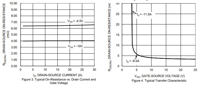
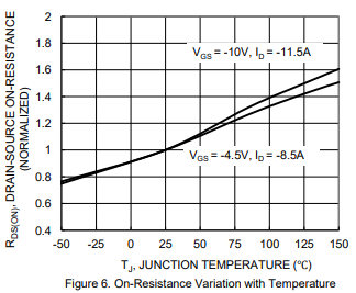
  1. The RDSon is specified at 25 degC. As the device heats up, it can increase by a factor of 1.5x. Depending on how hot you plan on letting your device get, that means that you could see up to 10-24 mΩ for your RDSon.

enter image description here

  1. The 7 mΩ resistance expects a Vgs of -10V. Your circuit permits a minimum input voltage of 5V (listed as 5-24 V in the schematic), which has a higher RDSon. At lower input voltages, you will have a RDSon that is up to 55% higher.

enter image description here

Can I dissipate this into the PCB

To be clear, the majority of the power is dissipated into the PCB already. Looking at the thermal resistance between the junction and ambient, a minimal SMT pad has 90 degC/W, while using 2oz copper and expanding the pad to use 1 in^2 for heat-sinking will reduce that to 47 degC/W.

enter image description here

Running the numbers with an ambient internal temperature of 40C and letting it always get hot enough to burn you (Tmax = 150C), that suggests a max of 2.3W with the PCB heat sink. Planning on running your devices this hot is a recipe for early failure. It's probably better to get a bigger MOSFET and run it cooler.

\$P_{max}=\dfrac{T_{Jmax}-T_{ambient}}{R_{\Theta JA}} = \dfrac{150^oC - 40^oC}{47 ^oC/W} = 2.3 W\$

\$\endgroup\$
6
  • \$\begingroup\$ the one im using has a 1.4W dissipation, i think this is the bigger package one. i definitely don't want it to get hot, does the thermal resistance scale linearly? so if i have 4 inch^2 of pcb it will be divided by 4 also ? \$\endgroup\$
    – Jake quin
    Commented Jun 7, 2021 at 16:32
  • \$\begingroup\$ what is your take on paralleling these mosfet if pcb space is a bit constraint? \$\endgroup\$
    – Jake quin
    Commented Jun 7, 2021 at 16:49
  • 1
    \$\begingroup\$ @Jakequin No, copper area is definitely something with diminishing returns. The expanded area is using the (thin) copper to spread heat out. Expecting 2W of power dissipation out of the PCB is already pushing it in my opinion. \$\endgroup\$
    – W5VO
    Commented Jun 7, 2021 at 16:50
  • 1
    \$\begingroup\$ @Jakequin You really don't have a way to guarantee that the current gets split evenly between the devices. Because of that, you don't have a good way of making sure that they both heat up the same. It's not going to run away on you since they will reach an equilibrium, but it's also not perfect. Don't expect doubling your devices to give you exactly double the power handling. \$\endgroup\$
    – W5VO
    Commented Jun 7, 2021 at 16:55
  • \$\begingroup\$ @Jakequin The limiting factor is, ultimately, how the PCB area dissipates heat. Splitting the heaters within the same area won't do much to the PCB temperature, since PCB-to-ambient thermal resistance is related to area only, it doesn't magically decrease just because you stick more devices on the PCB. If anything, more devices will shield the PCB more from the airflow and decrease its heat-dissipating capability! \$\endgroup\$ Commented Jun 7, 2021 at 17:38
9
\$\begingroup\$

Which revision of the datasheet are you using? I see 1.0 W listed for 25 degree ambient.

Anyhow, the PCB material itself if very bad at dissipating heat, you need copper planes to do anything.

The DMP3007 has a listed thermal resistance of 124 K/W with minimal copper area and 52 K/W with one square inch of copper. At 0.7 W and minimal area, you are looking at 86.8 degrees above ambient. That would call for a very cold ambient temperature to get any useful life out of your circuit. With one square inch, it's 36.4 degree above ambient, far more reasonable. Do you have room for 1 square inch on your PCB?

As for rising the current to 15 A, you need to consider all the limitations in the datasheet, thermal and continuous drain current. In your case, you are still limited by the thermals.

If it's a one off or small series, I would always recommend buying better silicon than hassle with heatsinks, fans and what not. If it's high volume product, you don't have this luxury.

\$\endgroup\$
3
  • \$\begingroup\$ Apoloies about the datasheet i forgot to link the part. Yes its a fairly large pcb so i have space, for this specific i am instinctually confident that the pcb copper can cool it down on how large it is. I just want to see how calculations is done, for the time i will encounter here im on limited space. \$\endgroup\$
    – Jake quin
    Commented Jun 7, 2021 at 15:58
  • \$\begingroup\$ the price of this fet is dirt cheap compared to the good ones, is it possible to parallel the p channels? is that a good idea? \$\endgroup\$
    – Jake quin
    Commented Jun 7, 2021 at 16:07
  • \$\begingroup\$ @Jakequin Yes it’s possible but you need one gate resistor per PFET. \$\endgroup\$
    – winny
    Commented Jun 7, 2021 at 16:43

Your Answer

By clicking “Post Your Answer”, you agree to our terms of service and acknowledge you have read our privacy policy.

Not the answer you're looking for? Browse other questions tagged or ask your own question.