1
\$\begingroup\$

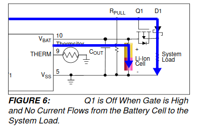
I was reading this application note from Microchip (AN1149) and I can't figure it out why this P-channel MOSFET (Q1) is placed like this:

  1. I thought the parallel diode integrated with the MOSFET will allow battery voltage pass to the load, why it isn't?

  2. I thought current through an p-channel MOSFET used as a switch goes from source to drain, but this appnote shows source is connected to the load an drain to the battery, why is that?

Regards!

\$\endgroup\$

1 Answer 1

1
\$\begingroup\$

From the schematic and the text, Q1 is there to prevent the external power from back-feeding the battery and screwing up the charge management.

So Q1 is supposed to be on when the external source is off.

The reason Q1 is "backward" is because a FET, by itself, is a pretty symmetrical device. The only thing that distinguishes source from drain is where the bulk connection goes -- that's what determines the direction of the internal diode. And in this case, a "normal" connection would cause problems when external power is applied.

So at the moment that the external power goes off, and the FET part of Q1 may or may not be on, the internal diode will conduct. Then when the FET does turn on hard, the diode will be bypassed.

When external power is on (and the FET off) the internal diode won't backfeed the battery.

\$\endgroup\$

Your Answer

By clicking “Post Your Answer”, you agree to our terms of service and acknowledge you have read our privacy policy.

Not the answer you're looking for? Browse other questions tagged or ask your own question.