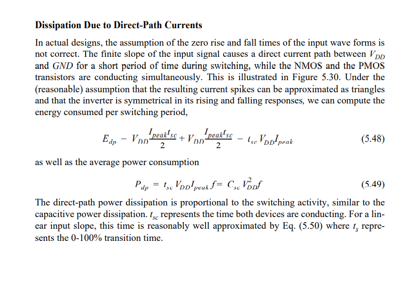
This is a snap from Chapter number 5 CMOS inverter, Digital integrated circuit by Jan M Rabaey .
I just wanted to know from where this \$I_{peak}\$ is measured. The direct path current exist till the output goes from \$V_{tn}\$ to \$V_{DD}-V_{tp}\$. But this current is peak value of which current? Current through the PMOS drain /source or the NMOS drain/source? While simulating which of the four currents should I take?

2 Answers
The current author talks about is the short-circuit current \$I_{sc}\$ relevant to transient power dissipation in a CMOS inverter.
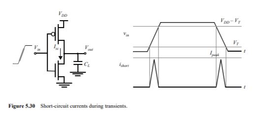
\$I_{sc}\$ flows from \$V_{DD}\$ to \$V_{SS}\$ when both PMOS and NMOS are conducting for a brief period of time while switching is happening at the input of the inverter. It is modelled/approximated as a spike within this time interval.
From the same book:
You can measure this current as the drain-source current through either PMOS or NMOS within the time interval where 'shorting' is happening. \$I_{peak}\$ is the peak value of \$I_{sc}\$.
A crude circuit to simulate the behavior of this current.
-
\$\begingroup\$ the current through PMOS and NMOS are different. So which one should I take? \$\endgroup\$ Commented Jul 6, 2021 at 18:40
-
\$\begingroup\$ @HariKrishna If the output is switching 1→0 you can measure it at the PMOS side, otherwise NMOS side. \$\endgroup\$– Mitu RajCommented Jul 6, 2021 at 18:55
-
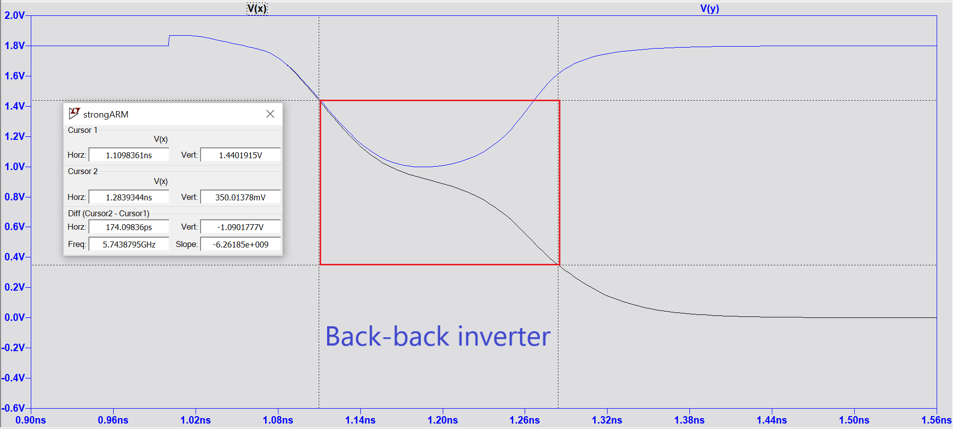
\$\begingroup\$ this is what I thought. But my actual issue just starts from this idea. So theoretically this will be from V<sub>tn</sub> to V<sub>dd</sub> - V<sub>tp</sub>. But then when input varies , it will take some time to reflect at the gate? Then the short circuit current duration will be different? Also my inverter is not going directly to gnd or vdd. It's having some increase then decrease, at that case from where should I measure ? @mitu \$\endgroup\$ Commented Jul 7, 2021 at 4:57
-
\$\begingroup\$ Okay delay can be neglected ? What about the increasing and decreasing ? To be precise , I used a back to back inverter. So in that input is varying from 1.8v to roughly 0.9V and later it goes back to 1.8v. So it's like vdd to 1/2Vdd and then back to Vdd. In that case what's the short circuit current l? \$\endgroup\$ Commented Jul 7, 2021 at 5:16
-
\$\begingroup\$ The back to back inverter was used in a Strong ARM latch \$\endgroup\$ Commented Jul 7, 2021 at 5:17
The peak current is the current need to charge (discharge) the gate of the MOSFET and it's mostly limited by the gate resistance and other parasitics (wiring inductance and various capacitances). In fact the gate current will also charge the parasitic gate-drain and gate-source capacitance (very important fact for power work, but it seems your book is about logic).
The basic idea about CMOS is that at rest nothing flows and bias current is almost null but during switch the gates need to be charged/discharged and that creates the dynamic dissipation which is the bulk of heat generation in CMOS logic (there's a little bit of cross conduction during switch, too).
The current spikes are not actually triangles but exponentials IIRC (the gates are more or less capacitors).
EDIT OOPS I read the question bad. Your peak current is actually the cross conduction between the CMOS pair. While one FET opens the other one is still closing so there is some VDD-VSS shoot through. It depends on the overlap of the switching curves of the P- and the N- channels
-
\$\begingroup\$ How do I find that current using simulation? I have been thinking about it for like 2 days. Still I am not sure which current is the short circuit/shoot throo/direct path current for which the peak is taken. Is it current through PMOS or NMOS? Some current through Mosfet is used to charge the capacitor. \$\endgroup\$ Commented Jul 6, 2021 at 18:44
-
\$\begingroup\$ just measure the drain current in one of the MOSFETs… during cross conduction it is substantially the same \$\endgroup\$ Commented Jul 7, 2021 at 11:19


