3
\$\begingroup\$

I need to draw a circuit from the following transfer function:
\$ \frac{V_o(s)}{V_i(s)}= - \frac{100}{(1+\frac{s}{\omega_{p1}})(1+\frac{s}{\omega_{p2}})} \$

I know how to derive a transfer function from a circuit, that part is easy. But wouldn't going the other way have waaaay more than just one solution. I don't even understand HOW or WHERE to begin. Any ideas?

\$\endgroup\$
2
  • \$\begingroup\$ Here is what I would do: Start by drawing the frequency and phase diagrams that go with the function. \$\endgroup\$
    – jippie
    Commented Feb 18, 2013 at 8:16
  • \$\begingroup\$ Electronics circuits very often (if not always) have different solutions for the same problem, nothing wrong with that. It gives you the opportunity to optimize different circuit properties than the initial problem, eg. for noise, power use, temperature stability, ... . It is often good practice to be able to explain why you made a particular design choice, but I expect that to be out of scope for the given problem. \$\endgroup\$
    – jippie
    Commented Feb 18, 2013 at 8:49

3 Answers 3

5
\$\begingroup\$

As jippie says, there is no single answer to this. But, think about the transfer function and how cascaded stages combine in (Laplace style) transfer functions. In this case, the transfer function is the product of 3 elements, gain, p1, and p2. Response of cascaded OpAmp stages will combine as the product of the stages. So, you could start by designing a 3 stage circuit with each stage carrying out one of the transfer function elements (gain, p1, and p2).

Look at how poles are formed by R and C combinations (Series or parallel) on the input of the OpAmp, and how they are formed by R and C combinations in the feedback path (between the OpAmp output and the negative input). Then you could look at ways to combine stages to end up with fewer stages (probably just one).

\$\endgroup\$
1
\$\begingroup\$

There are topologies very useful for placing poles where you want them, such as the Sallen-Key. Keep in mind when using these that capacitors don't have great tolerances, so avoid designs that require precision capacitances. http://en.m.wikipedia.org/wiki/Active_filter

\$\endgroup\$
1
\$\begingroup\$

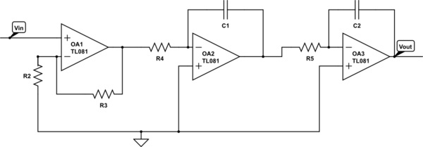
In accordance to what gsills said I will just go ahead and make the diagram for you, Think about this circuit. I will not specify the values of the Resistors and the capacitors.

schematic

simulate this circuit – Schematic created using CircuitLab

Think about how the transfer function of each functional block is related.

\$\endgroup\$
1
  • \$\begingroup\$ Functions are "first order" function, not integrator ... so use R1 // C1 and R6 // C2... \$\endgroup\$
    – Antonio51
    Commented Aug 30, 2021 at 9:34

Your Answer

By clicking “Post Your Answer”, you agree to our terms of service and acknowledge you have read our privacy policy.

Not the answer you're looking for? Browse other questions tagged or ask your own question.