1
\$\begingroup\$

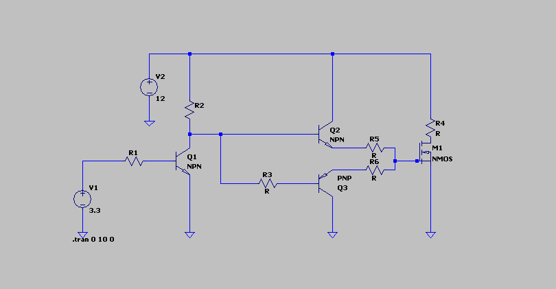
And by that title, I Mean that the drive current to the gate of the MOSFET when the BJT is on differs from the drive current for when it is off. I know that it would cause a difference between Toff and Ton but is there any other reason why it might be a bad choice? Let's assume you have an NPN transistor that can handle a much higher peak collector current than your PNP in the push-pull driver, would you still configure the BJTs so that they both have the same collector current even though your configuration is only bottlenecked by the PNP transistor? I would also want to know if asymmetrical driving can be used for buck converters.

Symmetrical drive:

Conventional symmetrical driving

Asymmetrical drive: R5 <<R6 (NPN can handle more current) Asymmetrical driving

\$\endgroup\$
5
  • 1
    \$\begingroup\$ Your title refers to MOSFETs, yet your body refers to BJTs, which are you concerned about? What's your application? Sometimes there are good reasons for asymmetrical drive, so it depends on what you are doing. \$\endgroup\$
    – John D
    Commented Aug 28, 2021 at 23:43
  • \$\begingroup\$ I am concerned about driving mosfest using BJTs, I just edited the title \$\endgroup\$
    – A.H.Z
    Commented Aug 29, 2021 at 0:10
  • \$\begingroup\$ @A.H.Z No schematic. But I guess you are talking about one quadrant being active while the other one is passive. I suspect that closed loop control may cover many ills. But without something specific I'm finding it difficult to say anything more. \$\endgroup\$
    – jonk
    Commented Aug 29, 2021 at 0:33
  • 1
    \$\begingroup\$ @A.H.Z I'm uncertain. You have a behavioral description -- it doesn't include the entire closed loop system of the buck converter. You are only focused on a BJT FET driver st age, which in both examples now show only 2-quadrant driving. When you write "asymmetrical" I perhaps thought incorrectly about active vs passive, when now I see you mean something different than I'd imagined before. That said, what is the rough ballpark of your needed currents? How fast is the on/off control taking place? \$\endgroup\$
    – jonk
    Commented Aug 29, 2021 at 1:58
  • \$\begingroup\$ It's not bad... \$\endgroup\$
    – DKNguyen
    Commented Aug 29, 2021 at 3:52

4 Answers 4

3
\$\begingroup\$

The only reason I can think of for requiring symmetry in the gates' charging and discharging currents is that you require some corresponding symmetry in the rise and fall (sink/source) characteristics at the output side of the MOSFET(s).

In the schematic you provide, for example, R4 is responsible for pulling up the drain voltage of the MOSFET M1, which means the rising of the drain voltage is limited entirely by R4 and whatever load is connected there. But M1 is on the low side, able to yank its drain potential to 0V pretty much instantly. So, in such a design, I might legitimately infer that you are concerned with fall time at the output (ability to sink current), but not so much with rise time. In that case it's far more important for you to switch on M1 as fast as possible, but you don't really care how long it takes to switch off. That's a rather contrived reason why gate drive asymmetry may be acceptable, but it illustrates the point.

If the load (R4) in your circuit were inductive, like a relay coil, there's a good argument for switching on M1 quickly, but off as slowly as possible, to control back EMF and the associated RF mess.

I would say that in most power applications, including DC-DC converters, you require the fastest on/off transitions possible, and to heck with symmetry. Anything to compromise that speed, including any resistance from driver to gate, is going to slow things down, and heat things up. The goal for MOSFETS switching power is to obtain the largest excursions of, and fastest slewing gate voltage possible, without breaking anything.

That's not to say symmetry is never a concern. (This is another contrived example, but off the top of my head, it's the best I have) If you need a low impedance source of harmonically pure square output, you would endeavour to match rising and falling output transitions, necessitating a gate driver built with deliberate effort to compensate for things like NPN/PNP disparity, or overshoot and ringing. I would expect to find such measures (more complicated than you have implemented with R3, but in the same vein) employed at the gates of output MOSFETs in laboratory equipment, like function generators, partly in an effort to produce as symmetric an output as possible.

On shoot-through

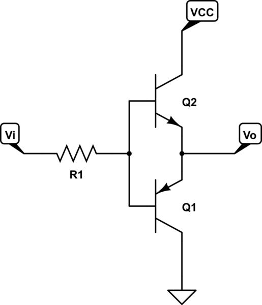
In response to A.H.Z's comment, on page 3 of this document the author states that to minimise "shoot-through" in a push-pull MOSFET pair, gate drive should be symmetrical. That's a somewhat sweeping statement, but it's not wrong, per se. This is referring to both voltage and time symmetry. Ideally you wish for one device to switch on at exactly the same time as the other switches off, which implies that each gate should be traversing its threshold at the same instant. This certainly implies temporal symmetry, but not necessarily voltage.

In the case of two MOSFETS whose gates are driven by the same signal, then you don't have much choice - I stick by my argument that the best medicine is to get that voltage from one extreme to the other as quickly as possible. If you have two MOSFETS whose gate threshold regions overlap somewhere between the supply rails, then that's marvellous, but the greater the difference in supply rail potentials, the less likely that is, the longer those two transistors will be conducting simultaneously, and every effort should be made to shorten that condition.

If however the gates are driven from separate voltage sources, timing becomes becomes a chief concern. If any delay causes one MOSFET to switch on before the other switches off, then you have problems. Having individual gate drivers for each transistor is really too complex a topic for a quick answer like this. A sweeping statement that "push-pull gate drive signals should be symmetrical" may be a good rule of thumb, but every application defines its own needs.

\$\endgroup\$
2
  • \$\begingroup\$ I agree perfectly on everything you said above , however this document seems to disagree with both of us, ww1.microchip.com/downloads/cn/AppNotes/… "MOSFET gate drive rise and fall times must be symmetrical, and as short as possible." \$\endgroup\$
    – A.H.Z
    Commented Aug 29, 2021 at 14:27
  • \$\begingroup\$ @A.H.Z I've updated my answer with my thoughts on that claim, which boil down to "in some cases, probably". \$\endgroup\$ Commented Aug 30, 2021 at 1:30
3
\$\begingroup\$

It's not 'bad' to have asymmetrical drive. In some cases it might be beneficial or necessary.

While your PNP may have a lower current capability or rating than the NPN, this current flows for only a brief time, so is unlikely to actually damage it. Secondly -- it's not a good idea (not very controllable) to limit a BJT collector current by limiting the base current -- that ratio is 'beta', and is one of the least controlled and variable parameters of the transistor.

If your MOSFET's load has any inductance (even the inductance of a long wire), turning it off too quickly (faster than microseconds in the case of just a long wire) may cause the wire's inductance to generate a potentially damaging spike at the drain of the FET. This is a reason to consider having slower turn-off than -on.

Your BJT circuit won't drive VGS to the full + rail -- you will lose about 0.7 V. Perhaps this is not a concern unless your supply is very low. On turn-off, it won't pull the gate quite down to 0 V -- it will rest at ~ 0.6 V for a while (and if you put a DMM or scope probe on it, that load resistance will make it go to 0 when it is connected.

Best to also put a small (unless the performance and other details are supplied, it's hard to get a most appropriate value) resistor; perhaps between 100 Ω an 10k between gate and GND.

\$\endgroup\$
3
  • \$\begingroup\$ I have taken into account all the possible disadvantages you mentioned above, for the hfe (or beta in dc) I've taken the lowest value the transistor could have from the datasheet and decided on the values of the resistance with a margin in mind , I do not understand the need to place a pull-down resistor to the gate however, the discharging part of the driver ( PNP transistor) should take care of discharging the gate,or is that not the case? \$\endgroup\$
    – A.H.Z
    Commented Aug 29, 2021 at 14:14
  • \$\begingroup\$ also the reason why I assumed it was bad was because of the emphasis of this document on the requirement of a symmetrical drive for buck converters. ww1.microchip.com/downloads/cn/AppNotes/… "MOSFET gate drive rise and fall times must be symmetrical, and as short as possible." \$\endgroup\$
    – A.H.Z
    Commented Aug 29, 2021 at 14:19
  • 1
    \$\begingroup\$ That document is misleading. There is no fundamental reason why rise & fall times must match. In some cases you NEED them to mismatch (when the effects of voltage spikes from parasitic inductances are considered). Similarly, you don't necessarily want them as short as possible -- that leads to voltage spikes also, and generally parasitic gate lead inductance in discretions MOSFETs means that you physically CAN'T drive the true gate faster than 5-10 ns. \$\endgroup\$
    – jp314
    Commented Aug 29, 2021 at 17:40
2
\$\begingroup\$

The Microchip article must be taken in context which is for a half-bridge driver (lower FET is used as a synchronous rectifier) for a buck switching power supply. They may be interested in controlling shoot through (where both FETs are briefly ON during the switching part). Your circuit needs will dictate what drive requirement is required.

\$\endgroup\$
1
\$\begingroup\$

"More and Less" are vague terms of generality and unless you have specifications for requirements cannot be discussed.

But let me make some assumptions for the benefit of the doubt.

The emitter follower a BJT used as a switch is Rout= Rb/hFE and the series R added is intended to equalize the source impedance differences of NPN vs PNP, so any differences won't matter.

Also consider common collector.

e.g. Rce is the BJT equivalent of RdsOn used as a switch. A PN2222A can be from 1 to 2 Ohms. A 2N290x can be 2 to 6 Ohms. This all depends on Ic/Ib current ratios and load current.

Rce= Vce(sat)/Ic These tend to be much higher than FETs for same cost or chip size. Although 10~50 mOhm is possible in BJT's these cost much more than FETs. But BJT pre-drivers can be cheaper. (2 cents )

The FET's gate has an equivalent input capacitance Ciss that is the Gate series resistance and shunt capacitance along with the Vds Miller capacitance. So driving with an Emitter Follower sees the highest current spike during transition through the threshold voltage. This value is inversely proportional to RdsOn in general, although there are many exceptions.

Any random web example you see may be sub-optimal lack of experience, money or experience extreme temperature rise or availability better parts. There may be good reasons for apparent odd choices too. No one will know any better without the full disclosure of assumptions,source of info, and lots of details.

Your experience will grow with good and bad examples. Use your discrete experience to identify what parameters are important to read in IC specs for Half-Bridges. These will usually perform better with guaranteed specs. The most important part of design is to make good specs before you choose anything.

\$\endgroup\$

Your Answer

By clicking “Post Your Answer”, you agree to our terms of service and acknowledge you have read our privacy policy.

Not the answer you're looking for? Browse other questions tagged or ask your own question.