-1
\$\begingroup\$

Here is a circuit- enter image description here

It has 2 parts, the first part generates a triangular waveform with pk-pk voltage of \$1.2V\$ approx. The second part is a CE amplifier with intended circuit gain of \$-10\$. The problem is that the simulation doesn't comply with my calculations. Here are my calculations-

a) Considering \$I_{c}=1mA\$ at the \$Q-point\$, \$V_{C}\$ for \$Q4\$ is set to \$4.5V(=0.5 V_{CC})\$.

b) This gives the value of \$R5\$ to be \$4.5k\Omega\$. I've used \$4.7k\$ due to availability issues, since I've to demonstrate this circuit as well.

c) This allows \$R6\$ to be around \$470\Omega\$, giving \$V_{E}\$ to be around \$0.5V\$.

d) \$V_{B}=1.2V\$ at the \$Q-point\$, thus.

Here are the detailed calculations-

a) Using resistors RC2/RC1 and the capacitors C12/C21, the time for charging the capacitors would be \$RC2*C21*ln(2)\$. This can be multiplied by 2, since values are the same, to get the time period, and hence the frequency.

b)For Q3, input impedance is \$47k\Omega\$ when input is high, and \$\infty\$ when input is low.

c)The thevenin equivalent output impedance for Q3 would be around \$1k\Omega\$ itself.

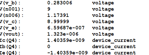
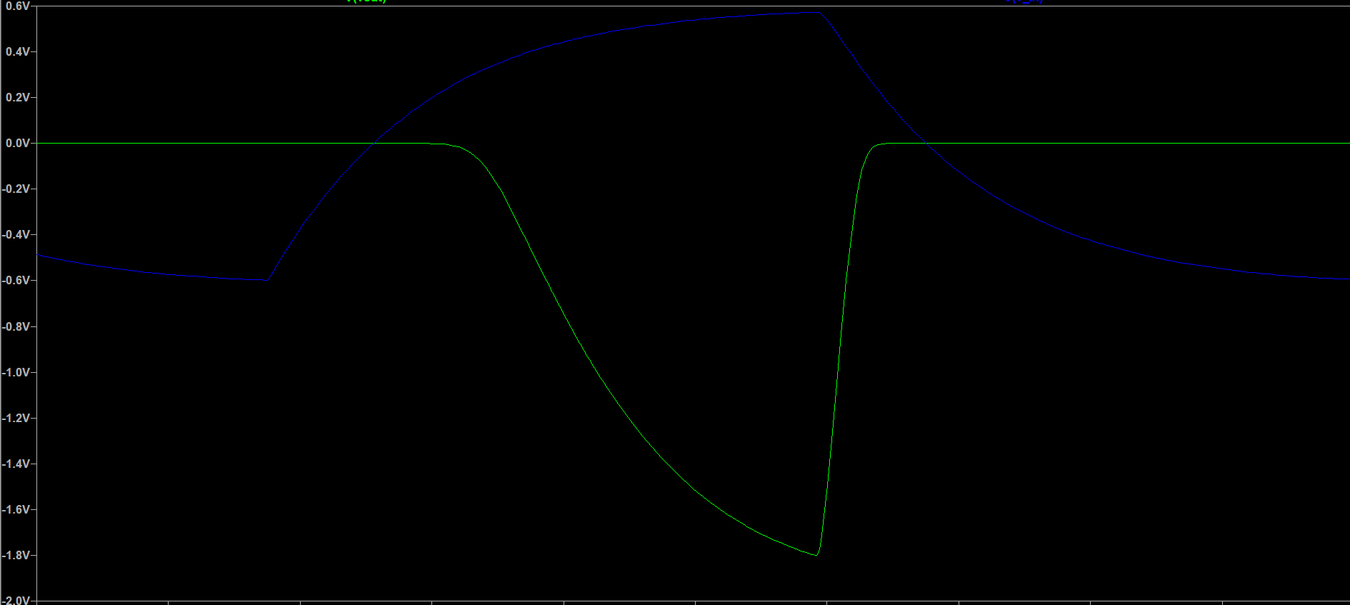
Using these, I expect a gain of -10 (opposite phase due to the negative sign), and thus around -6V. But, according to the simulation, I only get around -1.8V(a gain of around -3). Also, the quiescent values of \$Q4\$'s terminals do not match according to my calculations, nor does the quiescent collector current. enter image description here enter image description here
I don't realise where I'm going wrong horribly. Am I somehow neglecting the internal emitter resistance as seen by the base (\$=\beta r_{e}\$)? Should it be incorporated in the circuit gain? Can someone help me out in this?

\$\endgroup\$
11
  • 2
    \$\begingroup\$ Your schematic seems to be missing a junction between your biasing network R3/R4 and the base of Q4. This is also clear by the fact that LTSpice is showing you 2 different nets: "v_b" and "n006" with 2 different voltages - it wouldn't do that if they were connected. \$\endgroup\$
    – brhans
    Commented Sep 7, 2021 at 21:27
  • 1
    \$\begingroup\$ @electrovolt What's the frequency of that beast before Q3. You have a lot of frequency dependent parts after Q3's collector and you've written nothing about the rate. Besides that, I can't say that I see much by way of "calculations." (You write, "...do not match according to my calculations...") How may I point out a flaw if I don't see how you came to the idea that you can't predict what the simulator shows you? Don't you see how a lack of detail may be a small barrier in being able to help set you straight? \$\endgroup\$
    – jonk
    Commented Sep 7, 2021 at 21:57
  • 1
    \$\begingroup\$ @electrovolt You admit you can't predict what Spice is doing. I'll take you at your word on that. So, I may be not understanding you. Have you decided that you are right in your analysis and that Spice is wrong and you want us to tell you that? Or do you think that perhaps your willingness to gloss over details ("sails past all the filters used henceforth, creating no further problem") may be an issue? Just curious where you are mentally coming down on this question. I'd like to see your calculations. If you don't want to provide them, we may be at logger-heads. \$\endgroup\$
    – jonk
    Commented Sep 7, 2021 at 22:07
  • 1
    \$\begingroup\$ @electrovolt Well, if this was just a matter of not connecting a junction in Spice, and connecting it up makes things work for you, that's good. I don't need to see calculations if you are satisfied with them, already. Sorry I missed reading that detail. And yes of course it matters. How could it not matter??? \$\endgroup\$
    – jonk
    Commented Sep 7, 2021 at 22:26
  • 1
    \$\begingroup\$ Yeah, I've realized now @jonk. The problem is that while simulating the entire circuit, I completely overlooked that the base bias hadn't been created at all. \$\endgroup\$ Commented Sep 8, 2021 at 7:05

1 Answer 1

1
\$\begingroup\$

You neglected the input impedance Zin of the base to Re, as Zin = hFE*Re =~ 47k which is lowering the base bias. That's all.

Don't worry about hFE =100 unless you expect a 5% tolerance of Vc=Vcc/2 .there are better ways with negative feedback.

So what should 15k be increased to ? So that the effect in parallel with 47k results is 15k , as you intended.

To get Ic=mA, you must have Vbe= 600 mV to start with then add Re=470 mV you get around Vb=1V not 1.17

consider re is 26/Ic so for 1mA and subtract from Re. It would use 420 in this circuit and reduce 15k to 14k to get 1.0V on Vb.

But an NFB circuit is better.

\$\endgroup\$
3
  • \$\begingroup\$ Yeah, I had tried to set R4 to 22k instead of 15k, keeping in mind the input impedance, but the gain still doesn't change, according to LTSpice. \$\endgroup\$ Commented Sep 7, 2021 at 21:34
  • \$\begingroup\$ Yeah, I get it. But I'm new to electronics, so BJT's are the way to go right now. Would love to explore better circuits as I move on. \$\endgroup\$ Commented Sep 7, 2021 at 22:06
  • 1
    \$\begingroup\$ Try this tinyurl.com/yhlgn5xw Open loop gain about 80 and closed loop gain =1/2 Rc/ Rin at 1mA and Vc= 5V to allow for Vce +Ve saturation, \$\endgroup\$
    – D.A.S.
    Commented Sep 7, 2021 at 22:11

Your Answer

By clicking “Post Your Answer”, you agree to our terms of service and acknowledge you have read our privacy policy.

Not the answer you're looking for? Browse other questions tagged or ask your own question.