1
\$\begingroup\$

I am having some problems with understanding the following to apply it in different situations:

In order to reduce voltage strain on the primary switching transistor, we will assign 30% of the time to transformer charging, and 60% to discharging. This allows to perform the discharge at half the voltage level, so the switching transistor will only see 450 V instead of 600 V. Also this reduces peak current on the secondary rectifier, while increasing requirements for primary current handling and secondary voltage handling, both of which are not a problem in our supposed situation. The 10% of time remaining is there to account for time lost during switching, dead time of the controller, etc. At 100 kHz, our charge time will be 3 µs, and the discharge time will be 6 µs. A look into the ferrite's data table lets us know that at 100 kHz, maximum single-sided flux density should be limited to 0.1 T. Applying formulas 2 and 1, we quickly end up with the following:

300 V × 3 us ÷ 0.1 T ÷ 0.0002m2 = 45 turns

So, 45 turns will load up this core to 0.1 T in 3 µs, when applying 300 V. Nice and easy. On the secondary side we need 13.8 V, plus about 1 V for diode drop, giving about 15 V. We can use the same formula again, inserting the different values for voltage and time:

15 V × 6 µs ÷ 0.1 T ÷ 0.00002m2 = 4.5 turns

Did you like this? The turns ratio is 10:1, while the voltage ratio is 20:1, because the time ratio is 1:2!

Source: https://ludens.cl/Electron/Magnet.html

Does the 3 µs correspond to the rise time of the PD across the primary and does 6 µs correspond to the drop time of the PD across the primary or is it the time that must be "dead" where the primary has no current and so the magnetic flux contributed by the primary is currently zero for at least 6 us while the secondary is taking the magnetic flux that was stored and the dead time is any time where the PD is constant, either constant high or constant off? I do not understand how this rise time and drop time is controlled, is it purely a feature of the switching transistor or is it the fact of just using the time in the calculation means the number of turns selected forces that to be the charge and discharge times and as long as the times used fall with in the Frequency it would be clocked at we are good to go or something else?

How do I extended this concept when it is a full H bridge type topology? I understand I would have a division by 4 but if I state I want a 3 µs charge time and 6 µs discharge time can I still control it like this with a full H bridge, is the rise time in this situation the time to go from complete magnetization in one direction all the way to complete magnetization in the other direction and the discharge is the complete swing starting from the other side over the 6 µs or is the 6 µs the time their must be no magnetic flux from the primary side, so no current flow through primary for 6 µs before the signal continues on the rest of the way to recharging the magnetic flux in the opposite direction to where it came from? I would like to take advantage of the situation where the voltage change is higher than the turns ratio or does this only work with a flyback topology and only step down?

I hope that makes sense.

Thanks in advance.

\$\endgroup\$
6
  • 1
    \$\begingroup\$ Your question would be a lot more readable if you used a μ or two. \$\endgroup\$
    – Hearth
    Commented Sep 14, 2021 at 5:06
  • 1
    \$\begingroup\$ "0.000003 seconds" - use rationalized units please. \$\endgroup\$
    – Andy aka
    Commented Sep 14, 2021 at 7:02
  • 1
    \$\begingroup\$ @Andyaka I was told in school it was called engineering notation. Is rationalized units another name for the same thing? \$\endgroup\$
    – winny
    Commented Sep 14, 2021 at 8:37
  • \$\begingroup\$ @winny Maybe I should have said rational (or sensible) units. \$\endgroup\$
    – Andy aka
    Commented Sep 14, 2021 at 8:44
  • \$\begingroup\$ @Andyaka I’m not sure. English isn’t my first language so I’m asking. Not everything taught in school turned out to be correct. \$\endgroup\$
    – winny
    Commented Sep 14, 2021 at 8:49

1 Answer 1

1
\$\begingroup\$

That quoted article is about flyback converters: -

One very important example is the fly-back topology of switching power supplies.

So, when you say this: -

How do I extended this concept when it is a full H bridge type topology?

That makes your question about half a book too wide to cover. So, I'm going to ignore that request because a flyback converter and a full H-bridge converter are entirely different beasts and that makes your question much too wide to cover here along with your earlier questions on a flyback converter. You'll see in my answers below that you need to grasp the flyback converter in much more detail before looking at other topologies.

Does the 3 µs correspond to the rise time of the PD across the primary

No, the 3 µs corresponds with the ramping-up time of the current in the primary inductor when the main DC voltage supply is applied across the primary by the MOSFET when it gets activated.

does 6 µs correspond to the drop time of the PD across the primary

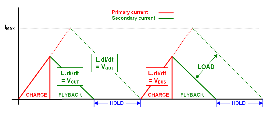
No, it corresponds with the secondary current in the inductor falling from the peak it attained (when the primary MOSFET deactivated) towards zero/low current. It can be regarded like this (for a 1:1 transformer operating in DCM): -

enter image description here

Picture from here for a DCM flyback converter. So the red waveform shows the current in the primary rising from zero to some peak value. Primary inductance and the supplied DC voltage generate the slope of that ramp (V/L).

If the transformer has a step-down ratio then the green secondary current waveform shown above is magnified by the ratio.

or is it the time that must be "dead" where the primary has no current and so the magnetic flux contributed by the primary is currently zero for at least 6 us while the secondary is taking the magnetic flux that was stored

For sure, when the primary MOSFET deactivates the primary current is theoretically zero but, the reflected voltage onto the primary from the current in the secondary will still be present.

I do not understand how this rise time and drop time is controlled

If you look at the diagram above and recognize that it's the current that is rising and falling in the primary and secondary and, then you recognize that the primary and secondary inductance along with the input and output voltage are all inter-twined then it should become clearer (eventually). This picture may help gel your thoughts about the voltages seen: -

enter image description here

\$\endgroup\$
1
  • \$\begingroup\$ Thank you, that helped a lot. \$\endgroup\$
    – axawire
    Commented Sep 14, 2021 at 22:19

Your Answer

By clicking “Post Your Answer”, you agree to our terms of service and acknowledge you have read our privacy policy.

Not the answer you're looking for? Browse other questions tagged or ask your own question.