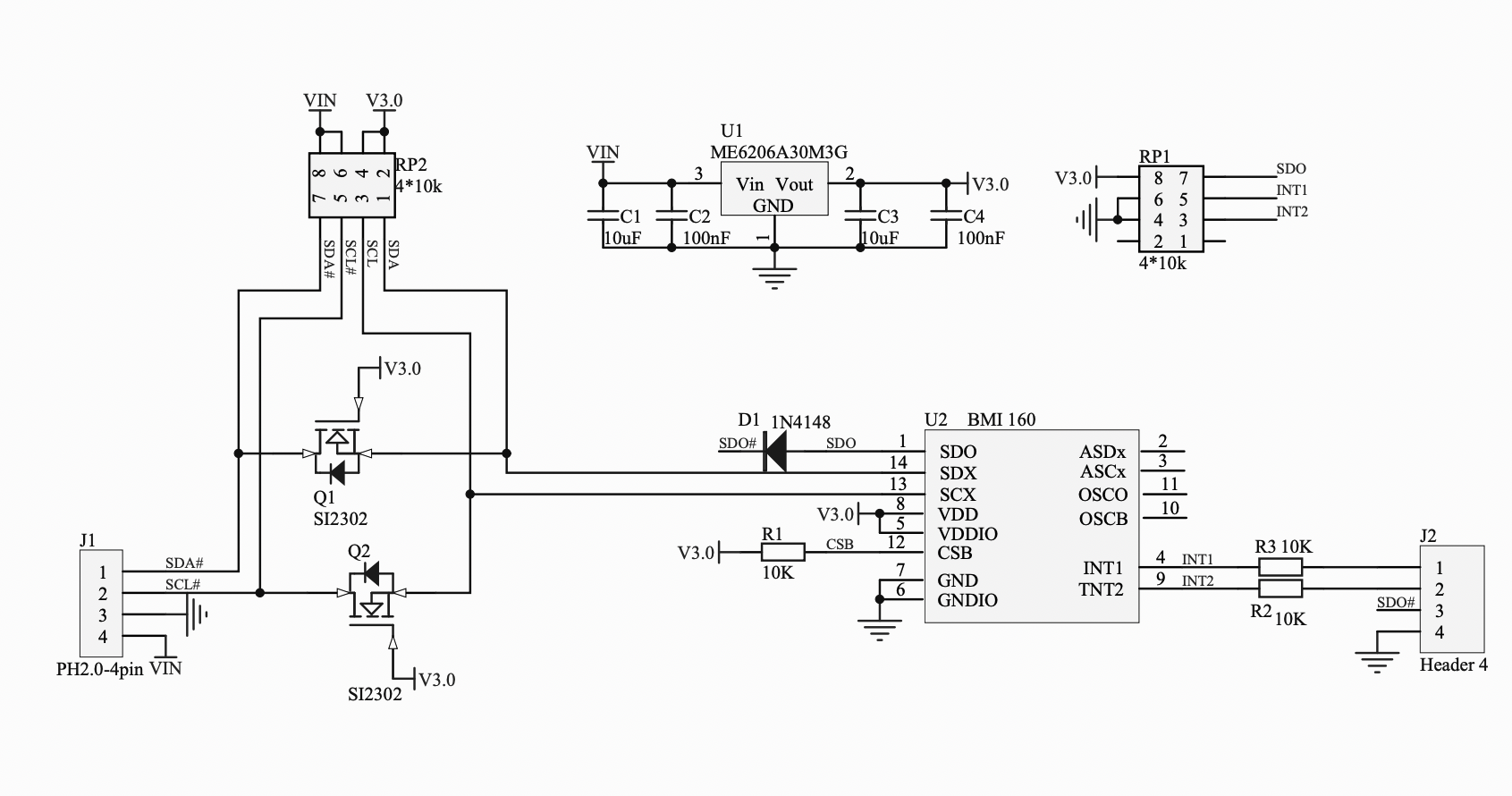
I am trying to make sense of these schematics. UI is an LDO which provides 3V output. Is it to isolate the BMI160 if there's not enough voltage?
1 Answer
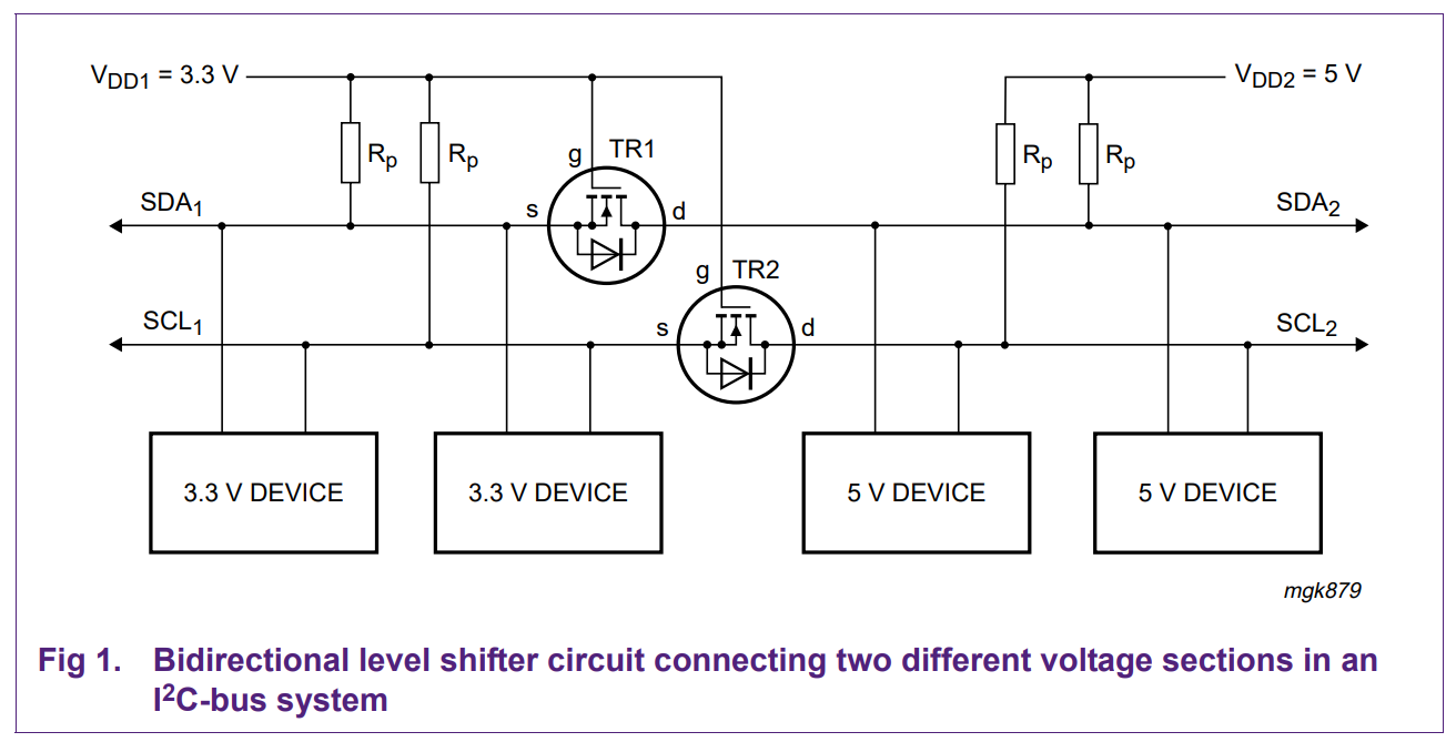
This is a bidirectional logic level adapter. Check the note AN10441 from NXP to get the full description.
It also allow to isolate a powered down bus section. Some current can indeed be injected into the chip from the communication lines via it's ESD clamp diodes, this circuit protect the chip from this behavior.
I often use this circuit with a pair of 100 ohms resistors on the SDA/SCL lines with a dedicated ESD diode to get the signals out of the board.


