0
\$\begingroup\$

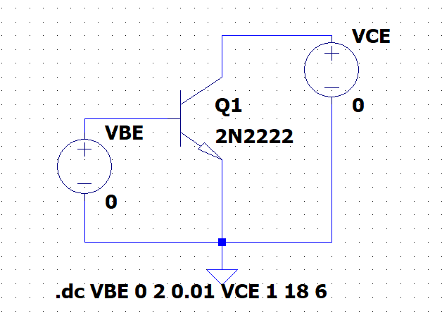
Let us assume that we have an NPN BJT sitting on the following circuit, drawn by LTSPICE: enter image description here

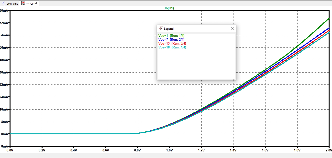
For the given dc sweeps we get base current versus V_BE for different V_CE values as below: enter image description here As we see for a fixed V_BE, increasing the V_ce will drop the base current. Qualitatively (no formula used) why this happens? I say when we increase the V_CE more electrons will be drifted to collector so I_C should go up and I_B is linearly go up as I_C going up since there is a beta coefficient relationship between base and collector currents. Where am I wrong in my reasoning?

\$\endgroup\$
6
  • 1
    \$\begingroup\$ Your reasoning is lacking as you don't actually understand much about the BJT yet. That ignorance is not a fault. In fact, Dr. Shockley himself missed it and it took a different Ph.D. to figure things out better, later. So don't take this harshly. There is no implied criticism intended. You could be brilliant and still miss it. So what do you understand about the depletion region as the collector-emitter voltage varies? Anything at all? Try to apply yourself to the question. See what you come up with. (I'd rather not steal this from you.) This is not a datasheet question, either. Just physics. \$\endgroup\$
    – jonk
    Commented Oct 12, 2021 at 6:41
  • \$\begingroup\$ I will try and be glad to learn about BJTs. \$\endgroup\$
    – Aria
    Commented Oct 12, 2021 at 6:58
  • 1
    \$\begingroup\$ Try to write out your thoughts. Just draw a nice, very simple diagram of the three regions. Keep in mind that the base region is "thin." And perhaps this answer here may help somewhat. \$\endgroup\$
    – jonk
    Commented Oct 12, 2021 at 7:20
  • \$\begingroup\$ Thanks, I thought about the depletion region and the effective base width and put my answer below. \$\endgroup\$
    – Aria
    Commented Oct 12, 2021 at 8:19
  • 1
    \$\begingroup\$ Good enough. I gave a +1 for it. \$\endgroup\$
    – jonk
    Commented Oct 12, 2021 at 10:05

2 Answers 2

4
\$\begingroup\$

The Base current in the NPN BJT has two components.

  1. The 1st component is due to the diffusion of holes from the base (p region) to the emitter (n region).
  2. The 2nd base current component is the one supplied by the external circuit to replace the holes lost by the recombination of the electrons already diffused from the n (emitter region). This current depends on the total minority charges (electrons from the emitter diffused to the thin base) in the base region. Since the total minority charges will increase linearly by the effective base width (which is the physical base width without the depletion regions), this 2nd base current component is linearly dependent on the effective base width.

Heart of the reasoning: As the V_CE increases the depletion region between base and collector grows making the effective base width narrower makes the 2nd component of base current smaller and the 1st component of the base current remains unchanged. Therefore increasing V_CE will narrow down the effective base width decreasing the base current as seen by LTSPICE simulation too.

\$\endgroup\$
1
\$\begingroup\$

You are neglecting power dissipation in this unrealistic test and for your region of concern the transistor would be burning up.

I cannot vouch for the LTspice model accuracy, but from datasheets for 2222A types;

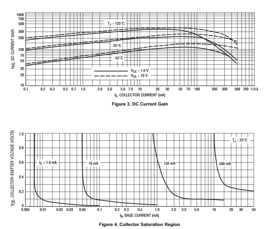
Vce Saturation (Max) = 1V @ 50mA, 500mA which dissipates 500mW which is far too much. Thus, Vce= 7V, 13V, 18V would not be possible in saturation.

Consider the PN2222A Rce is very good ( 1~2 Ohms @ Ic=10 mA) and Rbe you have shown reduces to ~ 17 Ohms.

That makes this hypothetical question a bit irrelevant. Also consider BJT's are Ic vs Vbe (not Ib vs Vce)

ref

https://media.digikey.com/pdf/Data%20Sheets/ON%20Semiconductor%20PDFs/MPS2222%20&%202222A.pdf

From above datasheet the saturation effects you can see for a nominal part Ic=500 mA, Ib=50 , Vce = 200 mV implies Rce=0.2/0.5 = 500 mohms @ 500 mA and 100mV/150mA= 667 mohms .

This causes the hFE to drop faster at high currents and Vce=1.0V due to the Rce effects in saturation, which does not occur at Vce=10 (dashed line plot) since that is not saturated.
enter image description here

You may enjoy reading the wiki page after the comment "This section may be too technical for most readers to understand" or prefer the modern lateral transistor MODELLA paper using voltage controlled conductance or synth [models][2] or the chapter by Dr. Chu with graphs, equations, base-drift, charge-control and the Kirk Effect or the NXP article on NEXTRAM models of vertical devices or the (guess how fast) "World's fastest transistor" and "yet another - 195 page book on - models can be fun"

Or maybe you just prefer the practical history of BJT's.
\$\endgroup\$
6
  • \$\begingroup\$ let us assume that we have a very efficient cooling \$\endgroup\$
    – Aria
    Commented Oct 12, 2021 at 5:26
  • \$\begingroup\$ Even with infinite heat sinks , it would exceed spec. and likely fuse the junction into a crystalized short circuit. \$\endgroup\$
    – D.A.S.
    Commented Oct 12, 2021 at 5:27
  • \$\begingroup\$ let us focus on vbe<0.9 V portion of the plot \$\endgroup\$
    – Aria
    Commented Oct 12, 2021 at 5:30
  • \$\begingroup\$ @TonyStewartEE75 "I cannot vouch for the LTspice model accuracy" -- well, it's a .model, so Gummel-Poon with floating points. :-) But LTspice also supports the MEXTRAM, so if anyone wants to translate this .model... \$\endgroup\$ Commented Oct 12, 2021 at 7:11
  • \$\begingroup\$ Yes @aconcernedcitizen but does the model show the >10:1 variance in hFE from process and device tolerances or NTC effects from Pd * Rja \$\endgroup\$
    – D.A.S.
    Commented Oct 12, 2021 at 14:52

Your Answer

By clicking “Post Your Answer”, you agree to our terms of service and acknowledge you have read our privacy policy.

Not the answer you're looking for? Browse other questions tagged or ask your own question.