1
\$\begingroup\$

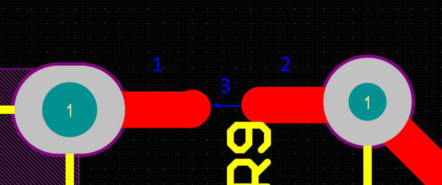
I want to route some tracks directly in the PCB file in Altium, So there is still no Netlist available.

enter image description here

So what rule/rules should I change to route pads directly, without applying the clearance rule between the track and the pad for the newly created nets?

\$\endgroup\$
4
  • 2
    \$\begingroup\$ Ascribe common net names to connected parts. Or better still, do that in the schematic level and do the job correctly instead of looking for non-ideal workarounds. \$\endgroup\$
    – Andy aka
    Commented Nov 2, 2021 at 14:30
  • \$\begingroup\$ This is not applicable due to the number of items to be connected. No schematic is present. \$\endgroup\$
    – Bavly
    Commented Nov 2, 2021 at 14:40
  • 1
    \$\begingroup\$ I found another solution which is to set the clearance between the track and pad to -1mm. and then (Design ---> configure physical nets). This will do the job perfectly. \$\endgroup\$
    – Bavly
    Commented Nov 2, 2021 at 14:41
  • \$\begingroup\$ Fact based answer was provided. Requirement was clear. Close-Open \$\endgroup\$
    – Russell McMahon
    Commented Nov 5, 2021 at 10:47

3 Answers 3

2
\$\begingroup\$

Disable Online DRC.
Preferences -> PCB Editor -> General -> Editing Options -> Online DRC = unchecked.

You should really create a schematic, even if there's only two parts on your board. In the time it took to write this question, you could have made your schematic. It's amazing how a seemingly simple project can go awry. By creating a schematic, you don't need to compromise design rules which are there to help you create a board without spacing and wiring errors. Plus, when you revisit this project in a year, a schematic will make more sense than a routed PCB.

\$\endgroup\$
1
\$\begingroup\$

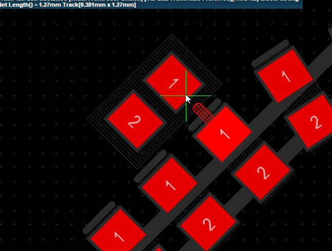
This is a couple of years old, but I came across this when searching for the same answer, I didn't find one, but I did come across a way of doing it that doesn't involve changing settings or creating rules that are in general not good.

  1. place a trace from the first connection to somewhere between the connections.
  2. place a trace from the second connection to somewhere between the connections.
  3. drag the copper from one connection onto the other.

enter image description here

\$\endgroup\$
1
\$\begingroup\$

There are two ways:

  1. Use Place - Line (or other shapes as you like) to draw arbitrary copper. It will be placed with Net = 'No Net'. Note that primitives will pick up nets when dragged or pasted onto other net objects (pads, existing traces, etc.), and will yield a shorted unconnected copper violation (with normal settings).

  2. Design / Nets / Edit Nets, and add new custom nets. You can construct the netlist manually this way (or edit a plaintext netlist and import it, just as well). Assign pads to nets in the dialog, or via their Properties. Route as usual; design checks will be meaningful.

  3. Add a schematic to the design, use generic symbols (headers say) if you have to, match up footprints and assign pins (you may need to create a PcbLib from the PcbDoc to be able to assign footprints), and continue as usual.

Note, if using schematic, once a synchonizable design is prepared, in PCB check Project / Component Links, and match up respective symbols/designators/footprints. This avoids renaming, swapping or deleting and re-adding that may occur with unsynchronized parts (part IDs not matched).

\$\endgroup\$

Your Answer

By clicking “Post Your Answer”, you agree to our terms of service and acknowledge you have read our privacy policy.

Not the answer you're looking for? Browse other questions tagged or ask your own question.