I would like to try to elaborate in detail how I think one should perform in detail practically impedance match between source and load via maximal power transfer using a L-matching network and whould like to know if my approach is correct.
Suggestion: I would like to describe now how I understood it and I would happy about any feedback on if I did it correct or wrong and how to repair it.
How I would do it:
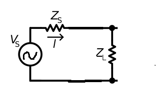
- We start with network consisting of source S with impedance \$Z_S\$ and load L with impedance \$Z_L\$. In general \$ Z_S \neq Z_L^*\$.
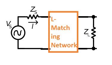
- What we do next. We put the L-matching network (the 'orange box') between source and load.
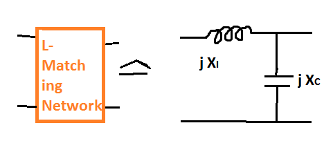
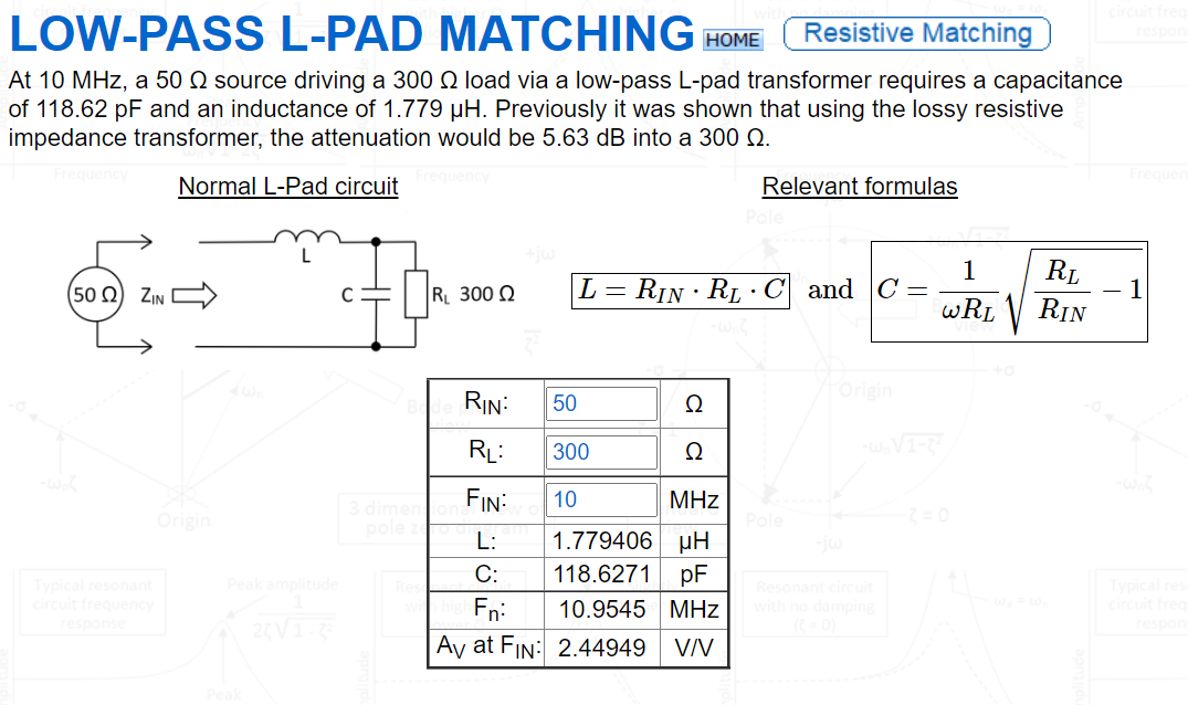
Internally a single L-matching network is a combination of a capacitor and a coil in one of the following possible configurations can be found eg here or there
Assume, we take the first one:
The reactances \$j \cdot X_C\$ and \$j \cdot X_I\$ of the capacitor and coil are not known and if we want to archieve an perfect match, these should be adapted.
Next, the most crucial part for me is which conditions should the satisfied by the still unknown \$j \cdot X_C\$ and \$j \cdot X_I\$?
My guess is that to determine \$X_C\$ and \$X_I\$ following equations should be satisfied:
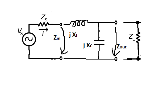
(I) \$Z_S = Z_{in}^*\$
(II) \$Z_{out} = Z_L^*\$
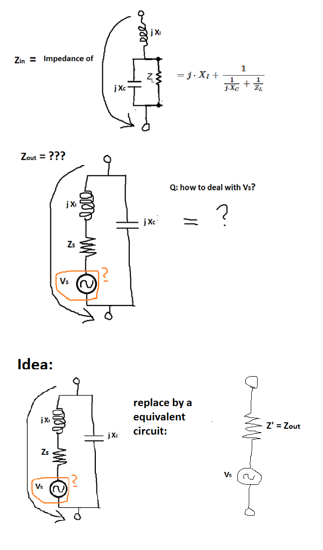
where \$Z_{in} \$ and \$Z_{out} \$ are following impedances:
So formally we are done at that point: \$Z_{in} \$ and \$Z_{out} \$ contain \$X_C \$ and \$X_I\$ as unknown variables and our task is to find \$X_C\$ and \$X_I\$ solving equations (I) and (II).
Questions:
A. Is in principle the procedure I have written done above to match impedance via L-matching network correctly explained?
B. If the answer to A. is positive, I'm not rather sure how to to express \$Z_{out} \$ in terms of \$ Z_S, X_C, X_I\$.
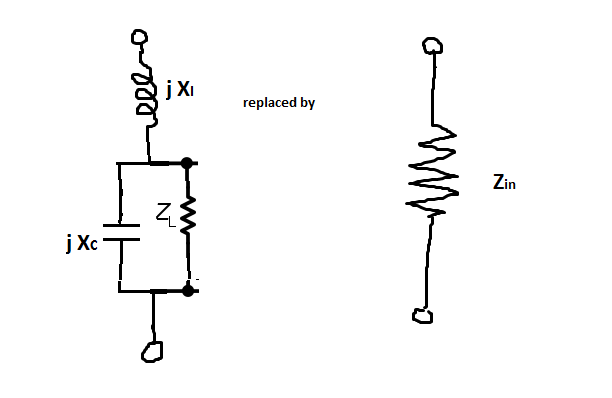
\$j \cdot X_{I} \$ is in series to parallel block of \$j \cdot X_{C} \$ and \$Z_{L} \$, which has impedance \$ \frac{1}{\frac{1}{j \cdot X_C}+ \frac{1}{Z_{L}}} \$, therefore
$$ Z_{in}= j \cdot X_{I}+ \frac{1}{\frac{1}{j \cdot X_C}+ \frac{1}{Z_{L}}} $$
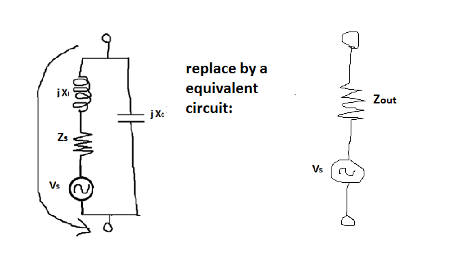
by construction. What is \$Z_{out} \$ in terms of \$ Z_S, X_C, X_I\$?
C. Can we play verbatim the same game if we want to reach minimal signal reflection instead of maximal power transfer (for example if our load is a transmission line) with small correction that everywhere we required \$ Z_A = Z_B^*\$ we replace by the conditions \$ Z_A = Z_B \$ but esle the the steps 1-4 go throgh? Is does this procedure above only works for maximum power transfer?
Addendum - respond to Andy's concern:
In your calculations you succeed in calculation of \$Z_{in} \$. As I said \$Z_{in} \$ by definition equals the impedance of the replacement circuit of:
and the missing impedance is \$Z_{out} \$ which should arise as:
It's not clear how your calculations below can be used / adapted to calculate \$Z_{out} \$.

