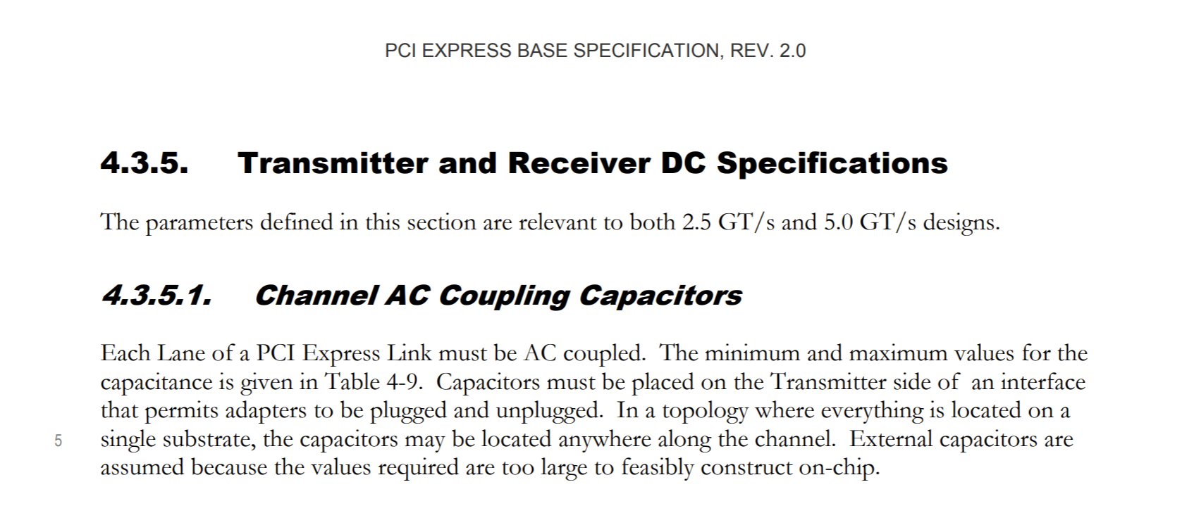
I'm working on implementing a PCIe 2.0 x2 system on a with a Xilinx Ultrascale. Reading through the PCIe 2.0 specification it requires 75-200nF AC coupling capacitors on the TX lines coming from the baseboard device. What about the clock lanes? Do those need to have coupling caps inline with them as well? I would guess it would be necessary but I can't find anything saying whether they are or aren't required for the clock lanes. 
1 Answer
There are PCIe devices out there, requiring AC coupling on the clock lanes as well. This is determined by the receiver, and the most common case is that AC coupling is not needed for the clock lanes.
If you are to use the FPGA as a PCIe slave device and the FPGA datasheet does not specify the clock lanes to be AC coupled, they should not be.
If you are using the FPGA as a master device, it is up to the slave to determine whether it needs AC coupling on the clock or not. When designing a base board with a PCIe connector, the base board should never have any AC coupling on the clock lanes. It should then be on the daughter board if the daughter board (receiver) needs AC coupling.
-
\$\begingroup\$ Exactly what I needed, thank you! In this case I'm using the FPGA as the root complex (master) and a daughterboard as the slave (endpoint). I'll leave off the capacitors on the clock lines. \$\endgroup\$– MitchCommented Dec 7, 2021 at 21:08
