0
\$\begingroup\$

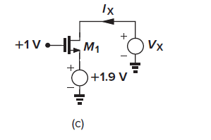
I am currently studying the basics of CMOS design and came across the following problem in Razavi's textbook with respect to a NMOS transistor :

enter image description here

The question is simple:

Let \$V_{SB}\$ = 0 (source-bulk). The voltage \$V_X\$ is swept from 0 to 3V and it is asked to plot the curve \$I_x\$ x \$V_x\$. Channel-length modulation effects are ignored for simplicity and the threshold voltage \$V_{TH}\$ = 0.7 V

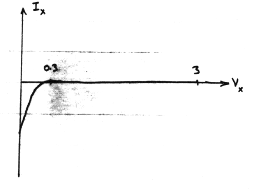
The answer graph, found in a hand-written solution manual has the following shape:

enter image description here

\$\textbf{My questions is}\$: How can M1, which is always under the \$V_{GS}\,< V_{TH}\$ rule (since \$V_{GS} = 1 - 1.9 = -0.9 < V_{TH} = 0.7)\$ conduct current?

I know CMOS technologies allow for a symmetric transistor thus letting current flow from source to drain and vice-versa, however I wouldn't expect current to flow when \$V_{GS} < V_{TH}\$.

Any help will be appreciated.

\$\endgroup\$
2
  • \$\begingroup\$ The symbol in your schematic is for a depletion-mode MOSFET. Are you sure that the problem doesn't assume depletion? If it was possible to swap the source and drain electrically then I think it would be misleading to explicitly mark one terminal as the source, as your schematic has done. \$\endgroup\$ Commented Dec 9, 2021 at 19:21
  • \$\begingroup\$ @ElliotAlderson The book hasn't stated any additional information regarding the mosfet, it's only depicted that MOSFET. \$\endgroup\$ Commented Dec 9, 2021 at 19:32

1 Answer 1

2
\$\begingroup\$

MOSFETs are symmetrical devices: Whatever channel contact has the lower voltage on it becomes the source. The labels you give them don't really mean anything. In your case, if Vx is zero, Vgs is 1V (and drain/source of the MOSFET are flipped). 1V is bigger than the threshold voltage, so the FET conducts.

Of course, if the bulk contact is connected to source, the symmetry is broken and you get an antiparallel diode (the body diode).

The same also works with bipolar transistors, by the way - you can operate a standard discrete NPN transistor with emitter and collector swapped. Of course, since bipolar transistors aren't constructed in a symmetrical fashion (the emitter is doped more), the gain and voltage rating of a flipped-around NPN will be much lower.

\$\endgroup\$
5
  • 1
    \$\begingroup\$ It's worth noting that planar FETs, FinFETs, and GAA-fets are usually symmetric, but the remark about gain/voltage rating being different can apply to some FETs (planar FETs with Lightly-Doped Drain and DMOS structures come to mind) \$\endgroup\$
    – nanofarad
    Commented Dec 9, 2021 at 19:16
  • \$\begingroup\$ So let me see if I understood. If the bulk were connected to the source, the MOSFET depicted in the figure would be always turned off, and the curve would be Ix = 0 all the way of Vx from 0 to 3v, is that right? \$\endgroup\$ Commented Dec 9, 2021 at 19:30
  • 1
    \$\begingroup\$ If the bulk is connected to the-terminal-marked-as-source then a PN junction is formed from the source/bulk to the "drain". If the "drain" is at a lower voltage than the "source"/bulk then the junction is forward biased and your MOSFET turns into a diode. For a N-MOSFET to flip its source/drain the bulk must always be at a lower voltage than either the source or drain (or at least below the PN knee voltage). \$\endgroup\$ Commented Dec 9, 2021 at 19:45
  • \$\begingroup\$ @ElliotAlderson I see. The terminals being flipped was the idea I was actually failing to understand but it seems clearer now. I have one last question though. I know I have no schematic to explain that, but : in a synchronous buck converter, during the moment the low-side mosfet is turned on, current flows from the "source" to "drain". From all that has been explained in this question, does it mean the "source" and "drain" are now flipped during that moment? \$\endgroup\$ Commented Dec 10, 2021 at 4:40
  • \$\begingroup\$ Yes, the FETs in a synchronous buck converter have to conduct current in both directions and the source's and drain's roles are technically flipped when they conduct in reverse. However, since these FETs also have their bulk contact connected to source, they're not quite symmetrical anymore - when switched off, they behave like diodes (from bulk/source to drain). Operating a FET both ways around is only possible when the bulk is connected to a lower potential (or when there is no bulk, as in JFETs). You'll actually find a note that the device can be operated in reverse in many JFET datasheets. \$\endgroup\$ Commented Dec 11, 2021 at 1:14

Your Answer

By clicking “Post Your Answer”, you agree to our terms of service and acknowledge you have read our privacy policy.

Not the answer you're looking for? Browse other questions tagged or ask your own question.