0
\$\begingroup\$

I'm using ICE40-16-WLCSP-Eval-Kit as a reference design for the Lattice ICE40-LP1K 84-QFN which I'm going to use in the motherboard I'm designing.

I did a little experiment with ICE40-16-WLCSP where I externally programmed the SPI Flash and saw that the FPGA is doing what I asked it to do (to blink the green led at a frequency of 2Hz).

The external programming was done using a Dediprog Flash Programmer.

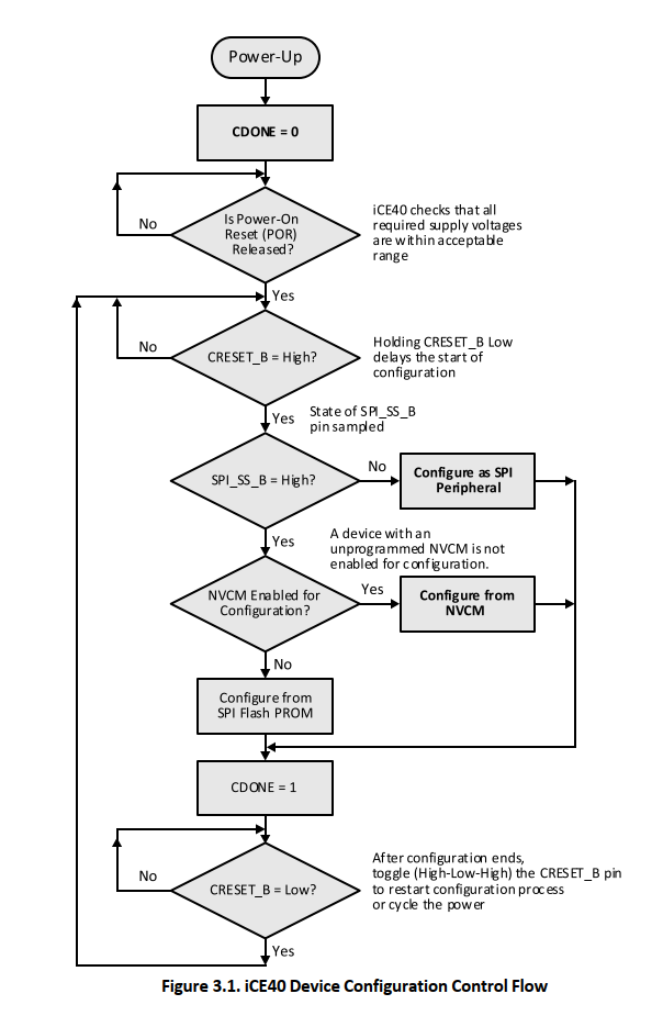
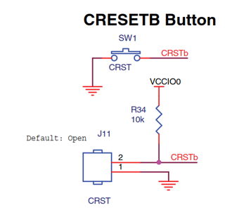
In order to see the effect of blinking the LED, I had to force a hardware reset pulse onto CRESET_B using a jumper on J11. I guess this is the last phase configuring the FPGA, according to this diagram:

enter image description here

enter image description here

Assuming ICE40-LP1K 84-QFN works at the same principle as ICE40-16-WLCSP, how can I perform this SPI programming without making a hardware reset?

The goal is to have as few manual operations as possible in the ATP process, for mass production.

I thought of connecting CDONE to a gate of a MOSFET transistor with its drain connected to CRSTb and the source to GND, but in this case I don't know how CDONE will behave. I would prefer that it gets asserted for short time only to perform the reset, but in this case it will be ON the whole time the FPGA is running after completing power up. How do I know this won't harm the FPGA operation?

I'm also open to other ideas to save up this hardware reset.

Note: CRSTb and CRESET_B are the same signal.

\$\endgroup\$
1
  • 1
    \$\begingroup\$ Please remove your 'update' and post it as answer for you to accept. Otherwise, the question will never be completed. By the way, it's 'load the configuration file and implement the design', not 'update the image and perform the code'. It a digital logic circuit, not a computer program to be carried out. Thanks. \$\endgroup\$
    – TonyM
    Commented Dec 13, 2021 at 14:33

1 Answer 1

1
\$\begingroup\$

The problem had been fixed. Turns out turning OFF and ON the Power does actually load the configuration file and implement the design. Apparently I didn't give enough delay time between the ON and OFF switches of the FPGA VCC Supply (maybe the capacitors didn't fully charge\discharge)

\$\endgroup\$
2
  • 1
    \$\begingroup\$ For future reference, this could be called race condition or be a part of a power-down-sequence to avoid this. \$\endgroup\$
    – winny
    Commented Dec 13, 2021 at 16:08
  • \$\begingroup\$ Thanks, turns out there is such tag called "race-condition". \$\endgroup\$ Commented Dec 13, 2021 at 16:11

Your Answer

By clicking “Post Your Answer”, you agree to our terms of service and acknowledge you have read our privacy policy.

Not the answer you're looking for? Browse other questions tagged or ask your own question.