0
\$\begingroup\$

I want make simple 1-bit memory using OR Gate like this picture

OR gate memory

It's working what I expect when using OR gate component. I change first input state to 1 so that it will give an output state of 1. Then the current output state which is 1 is carrying to second input of OR gate. Hence, it will give state 1 forever because, as we know, the OR gate will give result 1 if one or both input is 1.

I know there's no other way to make it output 0 unless we disconnect second input from the output.

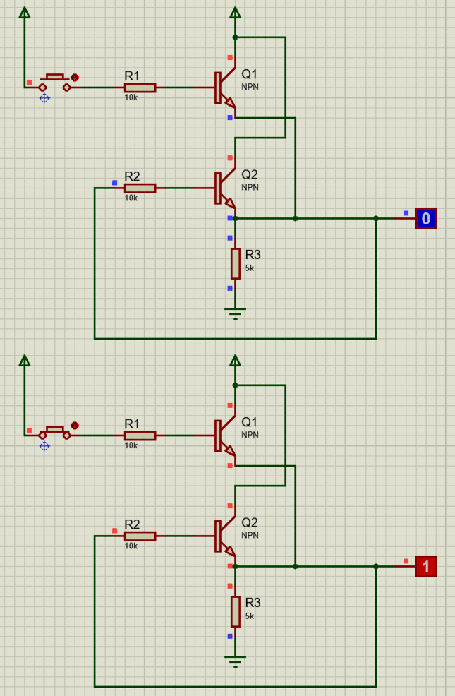
However, when I tried to make it, using transistors to create an OR gate, It's doesn't work. By that, I mean it doesn't save the state.

My configuration

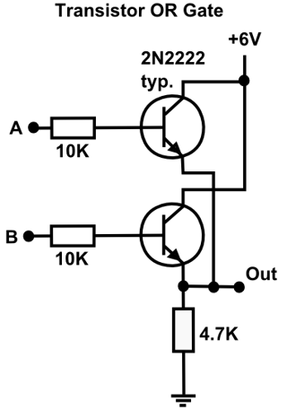
I'm just following configuration from internet like this. The difference is, I redirect the output to the second input.

Example from internet

So is there any other way how to reconfigure my transistor circuit to what I expect with OR gate memory?

\$\endgroup\$

2 Answers 2

1
\$\begingroup\$

Q2's base will be held at the same voltage as its emitter, but the base needs to be about 0.7 volts positive of the emitter for it to conduct.

Those simple two-transistor gates may have some use as a basic explanation of how a gate might work, but they won't work when combined in more complex logic circuits - the output of this sort of gate is not sufficient to drive another gate.

\$\endgroup\$
3
  • \$\begingroup\$ So any other way what should I reconfigure into TTL circuit so it will be what I expect. Maybe add some capacitor or what. \$\endgroup\$ Commented Jan 25, 2022 at 5:22
  • \$\begingroup\$ Look for the Texas Instrument datasheet for the 7432 - it has the internal transistor-level schematic of a TTL OR gate. It does have something close to your OR gate, but it is followed by an additional circuit to give output voltages that can drive the inputs of another gate. \$\endgroup\$ Commented Jan 25, 2022 at 5:50
  • \$\begingroup\$ @MuhammadIkhwanPerwira for this reason, an OR gate is often constructed as NOR + NOT. inverted gates (NOR/NOT/NAND) do increase the signal strength instead of decreasing it. \$\endgroup\$ Commented Jan 17, 2023 at 15:37
1
\$\begingroup\$

This is an example of Resistor- Transistor Logic or RTL which like Diode logic has slightly < 1 voltage gain and thus will not latch.

TTL on the other hand has a fan-out design of 10 for current or in other words a current gain of 10 by design and will support the original logic symbol expectation.

We expect logic to have a threshold and specified tolerances with variations in supply or temperature. This is somewhat like a comparator which ideally has very large gain. But gain and bandwidth we know are tradeoffs and so the gain is fixed for TTL to provide this tradeoff.

\$\endgroup\$

Your Answer

By clicking “Post Your Answer”, you agree to our terms of service and acknowledge you have read our privacy policy.

Not the answer you're looking for? Browse other questions tagged or ask your own question.