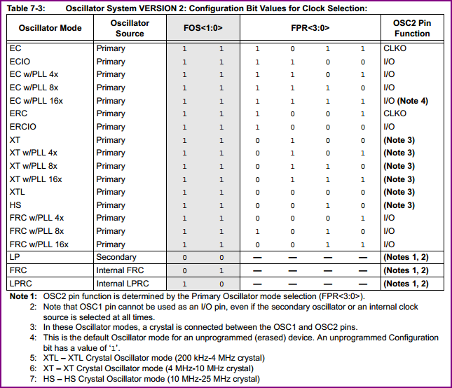
My question is about using FRC as an oscillator source and OSC2 pin as an I/O pin.
In several different manuals on dsPIC30F chips (ex: DS70139G, page 126) it is written:
   LP     Secondary       0 0 0   XXXXX  (Note 1, 2)
   FRC    Internal FRC    0 0 1   XXXXX  (Note 1, 2)
   LPRC   Internal LPRC   0 1 0   XXXXX  (Note 1, 2)

   Note 1: The OSC2 pin is either usable as a general purpose I/O pin or is completely
   unusable, depending on the Primary Oscillator mode selection (FPR<4:0>).
I carefully searched manuals, errata, forums, etc. But I cannot find clarification on how to set the FPR bits in the FOSC register to be able to use OSC2 as an I/O that the Note 1 suggests. Is this possible at all?
Errata on dsPIC30F3012 suggests using FRC with PLL and postscaler to make this pin useable (DS80448D - pages 3, 15). But this errata states that this problem is applicable only to revision B0, that is relatively old. We have chips of revision B1. Was this issue really fixed in B1? If yes, the work around should not bee needed, but in this case how this feature should be used?
Are there any differences in dsPIC30F3010 and dsPIC30F4011 devices regarding this issue?
I use assembler from XC16 v1.11. The sample code is (the part that sets FOSC):
.section    __FOSC.sec, code
            .pword    0xC701;         // FRC with 4x PLL.
Update:
I made experiments on programming undocumented FPR's into the device. As an environment I was using MPLABX and ICD3. It turns out that compiling always goes fine and the .hex file always contains the values that I put into the code. But some part of the tool chain blocks programming the undocumented FPR values into the device. After programming the "Configuration Bits" tabs shows the value C100 (FRC without PLL) and device works like this value is really programmed there.
The behavior described above (blocking programming) happens to majority of the values. The values 0x02, 0x04, 0x06, 0x08, 0x09, 0x0b, 0x0c manage to get through, but device does not seem to work properly.
These experiments have not destroyed the device.

