1
\$\begingroup\$

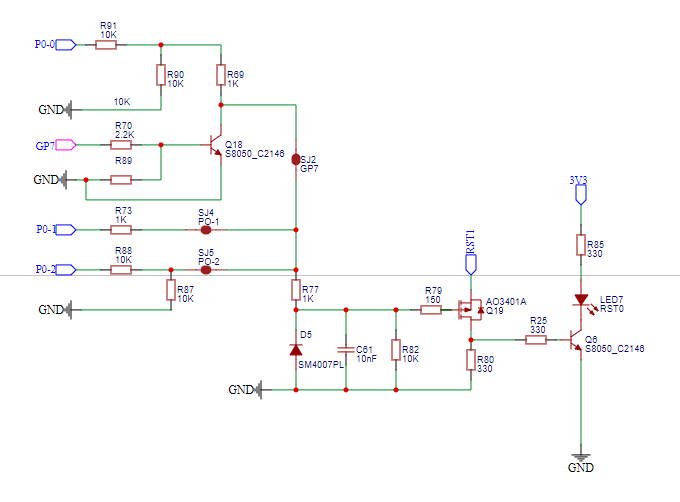
We have a reset circuit used in a peak-hold amplifier. Under normal conditions, a capacitor on the peak-hold circuit is grounded by RST1 (see circuit).

P0-0 is a fixed 24 V voltage from the supply.

When the peak hold is monitoring the ground is removed from the RST1 by adding a 3.3 V signal from an MCU to GP7, or by applying 24 V to P0-2, or by applying 12 V to P0-1. When 1 of the 3 events occurs the RST1 should float and LED7 should light.

I have not been able to get this to work and I do not know why.

Does the circuit look correct?

CIRCUIT

\$\endgroup\$
5
  • \$\begingroup\$ When you say the hold capacitor is grounded by RST1 do you mean RST1 is connected directly to the capacitor? If it is, it's not getting 'grounded' as there's the 330 ohm resistor in the way. The way you describe the inputs can't be correct, you say they are all active high, but GP7 goes through an inverter so it should work opposite of the other two inputs. \$\endgroup\$
    – GodJihyo
    Commented Feb 20, 2022 at 0:39
  • 2
    \$\begingroup\$ This circuit is drawn in about the most confusing way possible… It completely obfuscates the function of the circuit. Please redraw it in such a way that it’ll be obvious what the circuit is doing just by looking at it at first glance. \$\endgroup\$ Commented Feb 20, 2022 at 1:03
  • 2
    \$\begingroup\$ Further to above, have the gnd symbol pointing down, not vertical. There’s too much information missing to determine if the circuit is valid. \$\endgroup\$
    – Kartman
    Commented Feb 20, 2022 at 1:11
  • 2
    \$\begingroup\$ Instead of all that mess of analog signals interfering with each other, I'd recommend dividing all inputs to 3V and then using logic gate(s) to combine them as you need. With added benefit of using free gate on same chip to drive LED. The whole circuit can have less then half components of what it has now \$\endgroup\$
    – Maple
    Commented Feb 20, 2022 at 5:06
  • \$\begingroup\$ @GodJihyo When I say RST1 is grounding a capacitor I mean that it is ensuring that the capacitor in the peak hold circuit is discharged. This is why I cannot connect anything to RST1. the Mosfet Q19 has been working. \$\endgroup\$ Commented Feb 20, 2022 at 12:15

2 Answers 2

1
\$\begingroup\$

Let's simulate this thing:
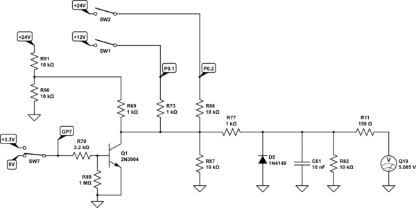
schematic

simulate this circuit – Schematic created using CircuitLab

Here's the "truth table" for the Q19's gate-to-ground voltage:

GP7 P0.1 P0.2 Q19.G
0V open open 5.1V
0V 12V open 9.4V
0V open 24V 8.7V
0V 12V 24V 10.2V
0V 0V open 1.3V
0V open 0V 4.0V
0V 0V 0V 1.2V
3.3V x x 0.0V

Since Q19 is a P-MOS, and the RST1 is the source potential, then none of those voltages will fully turn it on. The voltages would have to be negative for that. And, not knowing what the RST1 voltage range is, it's hard to even tell whether Q19 will ever get open. For example, at idle, if RST1 is above about 8V, it'll not be floating anymore.

Furthermore, Q19's drain will not reach ground, but about 1/2 of Q6's Vbe, so, let's say 0.3V.

So nothing much in this circuit is the way you'd want it to be.

Here's something that would work:
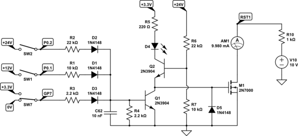
schematic

simulate this circuit

Q1 grounds the gate of the NMOS transistor M1, and floats RST1, whenever any of the inputs are high: be it GP7, P0.1 or P0.2.

The R6-R7 divider sets the gate voltage+0.6V when RST1 is to be grounded. The gate charges until no more current can flow through Q2.

Q1 is in series with Q2. When Q1 is on, Q2 turns on as well, turning the led D4 on whenever the NMOS is off and RST1 floats.

R5 sets the LED current.

R10, V10 and AM1 are only used in simulation, to indicate whether RST1 is grounded or open.

\$\endgroup\$
0
\$\begingroup\$

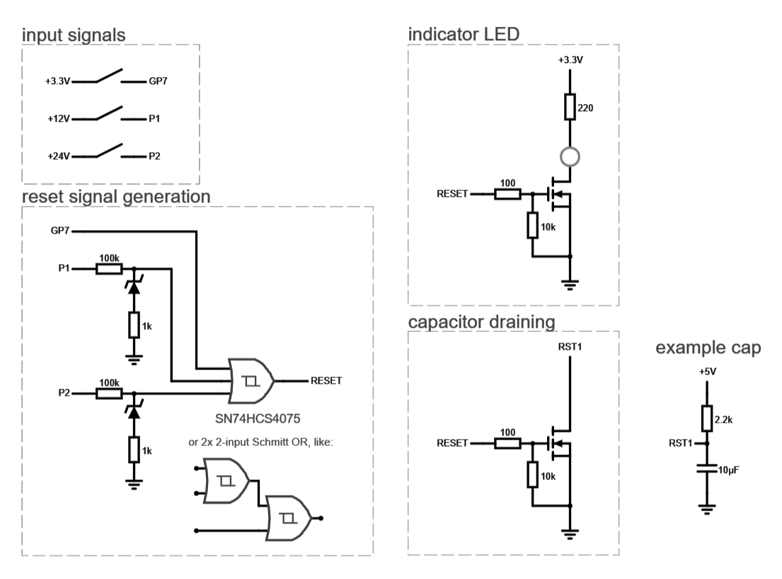
Based on your description, I'd go with something like this (simulation link):

Circuit diagram

The P1 and P2 voltages are clamped using 3.3V zener diodes to form logic level inputs. These, along with GP7, are fed to a 3-input OR gate with Schmitt trigger inputs, such as an SN74HCS4075. This generates the reset signal.

Alternatively, if you can't source the 3-input version, two 2-input Schmitt trigger OR gates can be chained to act like a 3-input gate. It should still end up being one chip as there's usually at least two gates in a single package.

The capacitor is drained by an N-channel FET, in the same approach you used in your design. The 100Ω resistor on the gate isn't really necessary for small transistors like AO3401, but it does help limit gate current on larger FETs.

The indicator LED is driven in the exact same way, and again the resistor on the gate isn't strictly necessary.

As others noted in the comments, it really helps to draw your schematic out in a way that makes it clear what each section is doing, using appropriate net labels and part orientation. Trying to keep voltage rails at the top, ground at the bottom, and signals flowing in the same direction (usually left to right) makes things much easier to read.

\$\endgroup\$

Your Answer

By clicking “Post Your Answer”, you agree to our terms of service and acknowledge you have read our privacy policy.

Not the answer you're looking for? Browse other questions tagged or ask your own question.