Question
"I'm mostly interested in how to explain the phenomena" -- JeanMi
That's a big question.
A real circuit isn't ideal. But it's almost always a good thing to first understand ideal circumstances. That way, a feel for what is fundamental about the circuit arrangement can be gathered. And from that vantage, the nonidealities can then be better seen and understood.
This isn't the only way to approach an understanding of all "the phenomena." But it is a good one.
Idealized Circuit
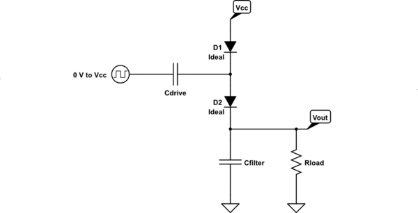
The ideal case is this:

simulate this circuit – Schematic created using CircuitLab
Before startup, \$V_{_\text{OUT}}=V_{_\text{CC}}\$ because ideal diodes \$D_1\$ and \$D_2\$ immediately charge \$C_{_\text{FILTER}}\$.
With that in hand, and assuming \$C_{_\text{DRIVE}}\$ is uncharged, then when the square wave input source starts at \$0\:\text{V}\$ then \$D_2\$ is off and \$D_1\$ is on and the voltage difference across \$C_{_\text{DRIVE}}\$ is immediately just \$V_{_\text{CC}}\$. When the square wave input source next moves to \$V_{_\text{CC}}\$, then \$D_1\$ is off and \$D_2\$ is on and and anode of \$D_2\$ would be at twice \$V_{_\text{CC}}\$ were it not for the presence of \$C_{_\text{FILTER}}\$ to absorb energy and therefore reduce the voltage difference across \$C_{_\text{DRIVE}}\$ to exactly \$V_{_\text{OUT}}- V_{_\text{CC}}\$.
Early, this difference is close to \$0\:\text{V}\$ and all of the energy stored on the drive capacitor is delivered, as the filter capacitor is still charging upwards. But eventually, an equilibrium is reached where the reduced energy delivered by the drive capacitor just matches up with the average energy consumed by the load, each cycle.
There will be ripple, as while \$C_{_\text{DRIVE}}\$ is charging \$C_{_\text{FILTER}}\$ must supply the load current. But we can temporarily ignore this issue by simply assuming that \$C_{_\text{FILTER}}\$ is large enough that we can ignore the question of ripple, for now.
The central point to focus attention towards is this question: How much energy does \$C_{_\text{DRIVE}}\$ deliver when the ideal system is at its equilibrium condition?
Energy Per Cycle
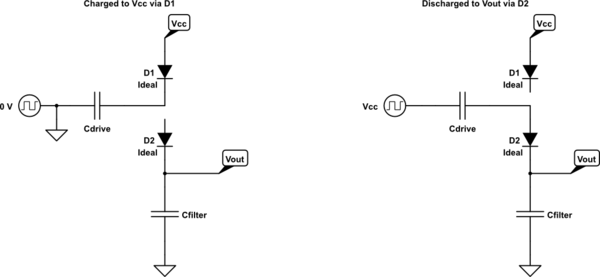
When in equilibrium, there are two states to consider:

simulate this circuit
On the left, the drive capacitor is charged up to \$V_{_\text{CC}}\$ via \$D_1\$ and has a charge of \$\left(V_{_\text{CC}}-0\:\text{V}\right)\cdot C_{_\text{DRIVE}}\$. On the right, the drive capacitor is discharged via \$D_2\$ into the filter capacitor and has a charge of \$\left(V_{_\text{OUT}}-V_{_\text{CC}}\right)\cdot C_{_\text{DRIVE}}\$. The difference between these is the charge that is lifted each cycle:
$$\begin{align*}
Q_{_\text{CYCLE}}&=\left[\left(V_{_\text{CC}}-0\:\text{V}\right)-\left(V_{_\text{OUT}}-V_{_\text{CC}}\right)\right]\cdot C_{_\text{DRIVE}}
\\\\
&=\left(2\cdot V_{_\text{CC}}-V_{_\text{OUT}}\right)\cdot C_{_\text{DRIVE}}
\end{align*}$$
The amount of charge lifted times the lifted voltage height is the energy delivered. In this case, as the charge is lifted from the ground reference up to \$V_{_\text{OUT}}\$, the energy lifted is:
$$\begin{align*}
E_{_\text{CYCLE}}&=Q_{_\text{CYCLE}}\cdot\left(V_{_\text{OUT}}-0\:\text{V}\right)
\\\\
&=\left(2\cdot V_{_\text{CC}}-V_{_\text{OUT}}\right)\cdot C_{_\text{DRIVE}}\cdot V_{_\text{OUT}}
\\\\
&= V_{_\text{OUT}}\cdot\left(2\cdot V_{_\text{CC}}-V_{_\text{OUT}}\right)\cdot C_{_\text{DRIVE}}
\end{align*}$$
(That's also the same as \$E_{_\text{CYCLE}}=2 \cdot\left(\frac12 C_{_\text{DRIVE}}\left[V_{_\text{CC}}\right]^2-\frac12 C_{_\text{DRIVE}}\left[V_{_\text{OUT}}-V_{_\text{CC}}\right]^2\right)\$ if you prefer to see it that way.)
Power
We are now at a point where we can make a statement about power. The power is just energy per unit time. And the time per cycle is \$t_{_\text{CYCLE}}=\frac1{f}\$. So the equilibrium power condition is easily stated as \$P=\frac{E_{_\text{CYCLE}}}{t_{_\text{CYCLE}}}=f\cdot E_{_\text{CYCLE}}\$.
Obviously, this must match up with \$\frac{\left[V_{_\text{OUT}}\right]^{2}}{R_{_\text{LOAD}}}\$ in the equilibrium state. So:
$$\begin{align*}
f\cdot E_{_\text{CYCLE}}&=\frac{\left[V_{_\text{OUT}}\right]^{2}}{R_{_\text{LOAD}}}
\\\\
f\cdot V_{_\text{OUT}}\cdot \left(2\cdot V_{_\text{CC}}-V_{_\text{OUT}}\right)\cdot C_{_\text{DRIVE}}&=\frac{\left[V_{_\text{OUT}}\right]^{2}}{R_{_\text{LOAD}}}
\\\\
f\cdot \left(2\cdot V_{_\text{CC}}-V_{_\text{OUT}}\right)\cdot C_{_\text{DRIVE}}&=\frac{V_{_\text{OUT}}}{R_{_\text{LOAD}}}
\end{align*}$$
That can be solved for \$V_{_\text{OUT}}\$ as:
$$V_{_\text{OUT}}=2\cdot V_{_\text{CC}}\left[\frac1{1+\frac1{f\,\cdot\, C_{_\text{DRIVE}}\,\cdot\, R_{_\text{LOAD}}}}\right]$$
And here you can now see why it is important that \$f\cdot C_{_\text{DRIVE}}\cdot R_{_\text{LOAD}}\gg 2\$. You want the term, \$\frac1{f\,\cdot\, C_{_\text{DRIVE}}\,\cdot\, R_{_\text{LOAD}}}\$ to be small with respect to 1 if you want the output voltage to approximate a doubling of the source voltage.
You can also solve it for \$C_{_\text{DRIVE}}\$ to get:
$$C_{_\text{DRIVE}}=\frac{1}{f\,\cdot\,R_{_\text{LOAD}}\cdot\left(2\cdot\frac{V_{_\text{CC}}}{V_{_\text{OUT}}} - 1\right)}$$
Moving Still Further
There's a lot more to deal with, while staying with ideal cases. For example:
- What's the equilibrium behavior of \$V_{_\text{OUT}}\$ when the filter capacitor is not arbitrarily large? A quantitative answer to this question allows specifying a peak-to-peak ripple; using that specification to then size the filter capacitor, entirely independently from the size of the drive capacitor.
A thought to consider here is that \$E_{_\text{CYCLE}}\$ is delivered instantly (ideal case), so the filter capacitor supplies the required current for the entire remainder of the cycle, not just half of it or some other fraction.
The implications of such a consideration should be to expect that the output voltage will look like, in the ideal case but with ripple now included, a sawtooth.
This is then a prediction.
Getting back to the point, the question about the equilibrium behavior of \$V_{_\text{OUT}}\$ can be directly addressed while still keeping ideal diodes and an ideal voltage source for the clocking input. And it introduces another design parameter.
This gets to another prediction that can be made. Since the drive capacitor can be sized only by considering the desired average output voltage, the frequency being used, the supply voltage rail value, and the load, it would seem that the size of the filter capacitor doesn't matter -- except as it applies to the output ripple magnitude. So we should be able to find this result, too.
We now have at least these two predictions beyond where we started, with respect to the equilibrium situation of the ideal case:
- The drive capacitor is determined by the single-supply source voltage, the frequency used, the size of the load, and the desired average output voltage. The drive capacitor does not impact the output ripple, which is independently determined by the filter capacitor.
- Conversely, the filter capacitor value has no influence on the output voltage. It only affects the peak-to-peak ripple voltage seen by the load.
- With a finite size filter capacitor, the output voltage should appear as a sawtooth shape (with its "teeth" having an exponential decay edge to them if the filter capacitor is small enough to make that become more evident.)
I haven't discussed the formula for establishing the size of the filter capacitor. But given #3 above, it is very easy to work out by the simple application of: \$I_{_\text{C}}=C\frac{\text{d}V_{_\text{C}}}{\text{d}t}\$.
If you think there's not more to find in the ideal case in equilibrium and with ripple added, think again. There is a subtle effect due to ripple, once that is injected into one's viewpoint. This is the fact that the drive capacitor cannot completely discharge, as earlier assumed, at the instant of the rising clock edge. This is because the drive capacitor design is based upon the average output voltage. So, if ripple is considered, half of it will be above the average and half below. So on the rising edge most of the charge may be released by the drive capacitor. But not all of what was expected. That will have to slowly "dribble" out as the load gradually pulls down the filter capacitor. (And, in fact, the drive capacitor will continue to supply charge after the average is met because as the load continues to lower the filter capacitor voltage, the drive capacitor will be able to supply still more charge.)
There are always these kinds of refinements to a view. You start simple and work out the details. Then you find, when you look more deeply, there's yet another effect that you'd earlier missed. And so on.
But until you know the larger picture (in this case, that the drive capacitor discharges mostly at the rising edge) and can understand most of the experimental result, you cannot see more deeply into these new effects.
In science, this is a matter of studying residuals. Each time you think you understand something well, you find that you do. But that there still remain some unexplained residuals. So you now focus on those and study them until you gain some insight into one of the causes. You separate out that effect, after more study and thinking about it, and add that knowledge to the prior knowledge to make still better predictions. Then you find there are still more, but smaller now, remaining residuals. And you study those. Etc.
After you have worked out how to size these two capacitors, you can work on nonidealities; such as limitations in the clocking source's current compliance (or impedance) and diode voltage drops and bulk resistance, among others. You might choose to approach these from an energy loss consideration. Or choose a different approach. Up to you.
A Summary for Now
I hope this approach has achieved two things: (1) Provided some clarity of mind about the ideal situation, from which to begin including nonidealities; and, (2) Illustrated how to deduce theory into specific situations.
In this latter case, it's important to take note of something. I could have blindly applied a quantitative calculation, cross-pollinated from some other circumstance, and used \$\frac12 C V^2\$ directly to the drive capacitor and gotten a wrong answer in doing so. That's because that formula was derived from theory into a different circumstance.
When facing each situation, you need to first decide whether or not the boundary conditions that were used to develop some other formula still apply to the new circumstance. If not, then set the formula aside and re-examine the new case using the same theory as before but now deducing it into the particular circumstance, at hand.
Theory is always right. It's just not quantitative. Theory expresses meaning and relationships. But each circumstance has to be taken into account, when applying theory, in order to develop an appropriate quantitative expression for that particular circumstance.
This is one of the hazards that catches lots of people (including me), unawares. It's all too easy to apply well-worn formulas to new circumstances without taking a moment first to see if they may still apply.
So I want to haul this out in front of you so that it's something you'll remember and keep to heart. General physics theory just works. But it has to be deduced into experimental circumstances in order to generate quantitative prediction for that experimental setup.
Hopefully, this sets things up to allow you to see just a little better and a little further and illustrates an approach towards analyzing the circuit and to develop still further towards a more managed and practical design approach.
Left to you, for now, is to think about how close (or far) from ideal that a practical circuit really is. How much will part variations matter? How sensitive is the circuit to part variations as a function of the selected output voltage (relative to ground) versus the clocking source voltage difference? Does selecting a lower output voltage reduce part variation sensitivity? Or increase it? Etc.
Obviously, part variations can matter a great deal if badly chosen. But the question is more about how much they matter when they are well-chosen. Is there still a wide variation? Or does the design come under enough good management that multiple instances of the same design will provide reasonably predictable results?
With my best wishes...
Validating Simulations
I thought I'd now finally add some simulations to test the above claims about the equilibrium condition for the ideal case.
A nearly ideal diode can be fabricated for simulation from this Spice card:
.model IDEAL D(Vfwd=1u, Ron=1u)
The forward voltage is only a microvolt and the on-resistance is a microOhm.
I'll also use a .TRAN simulation card that specifies the capture of the simulation only after the equilibrium condition has arrived. I'll use a clocking frequency of \$10\:\text{kHz}\$, so I believe waiting a couple of seconds should be sufficient and that we only need to see about \$10\:\text{ms}\$ worth of data -- about 100 cycles. The .TRAN card I've chosen is this:
.tran 0 2 1.99 1u
I'll also use a \$10\:\text{V}\$ input source voltage supply rail value.
I want to use a clocking source that runs with about 50% duty cycle, so as to highlight and illustrate the effect when the drive capacitor continues to supply a little charge during half the cycle.
I'll run the following cases, first:
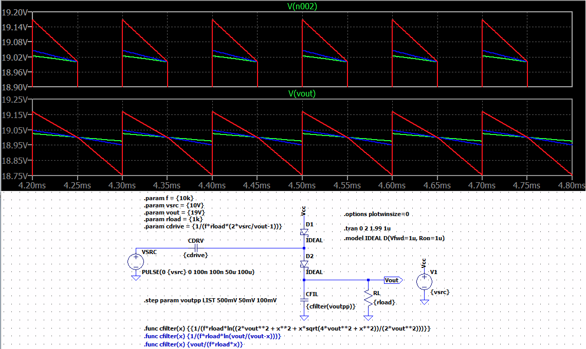
- \$V_{_\text{OUT}}=19\:\text{V}\$, \$R_{_\text{LOAD}}=1\:\text{k}\Omega\$, \$V_{_{\text{OUT}_\text{PP}}}=500\:\text{mV}\$
- \$V_{_\text{OUT}}=19\:\text{V}\$, \$R_{_\text{LOAD}}=1\:\text{k}\Omega\$, \$V_{_{\text{OUT}_\text{PP}}}=50\:\text{mV}\$
- \$V_{_\text{OUT}}=19\:\text{V}\$, \$R_{_\text{LOAD}}=10\:\text{k}\Omega\$, \$V_{_{\text{OUT}_\text{PP}}}=100\:\text{mV}\$

You can see the "subtle" effect I mentioned, earlier, where the drive capacitor's charge is mostly disbursed at the rising edge, but not all, and it is allowed to continue supplying charge for half of the cycle (slowly trickling in.) The effect is less noticeable when the ripple is less, of course. But this shows all of the impacts and you can easily see a "kink" in the output voltage with the largest ripple (the red curve) when the clock reaches 50% and moves back to ground.
Now let's lower the output voltage:
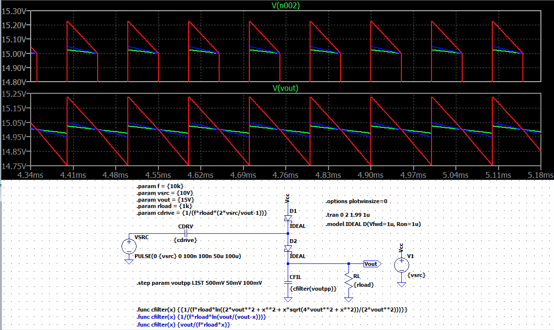
- \$V_{_\text{OUT}}=15\:\text{V}\$, \$R_{_\text{LOAD}}=1\:\text{k}\Omega\$, \$V_{_{\text{OUT}_\text{PP}}}=500\:\text{mV}\$
- \$V_{_\text{OUT}}=15\:\text{V}\$, \$R_{_\text{LOAD}}=1\:\text{k}\Omega\$, \$V_{_{\text{OUT}_\text{PP}}}=50\:\text{mV}\$
- \$V_{_\text{OUT}}=15\:\text{V}\$, \$R_{_\text{LOAD}}=10\:\text{k}\Omega\$, \$V_{_{\text{OUT}_\text{PP}}}=100\:\text{mV}\$

In this case, there's much more margin so a much larger percentage of the drive capacitor's charge is disbursed immediately and now the shape of the output voltage with the highest ripple doesn't show much of a kink in it. The top diagram does show the fact that the drive capacitor does continue to trickle charge, as before. But the impact is less noticeable on the output curve, now.
Above, I magnified this subtle effect by choosing a 50% duty cycle. An advantage of doing that is that the formula used to size the drive capacitor was developed on the idea of the average output voltage and so the simulator above does show that this average value is roughly achieved, as predicted. The price of doing that, though, is that the drive capacitor continues to supply charge for a while and a "kink" can be seen in more extreme ripple cases.
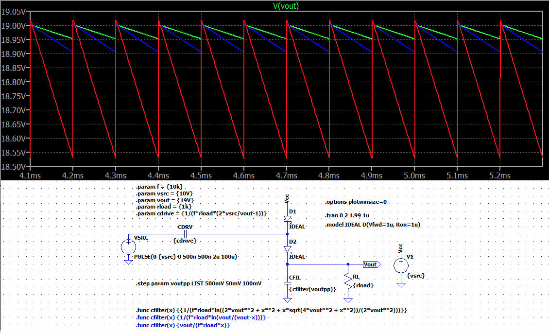
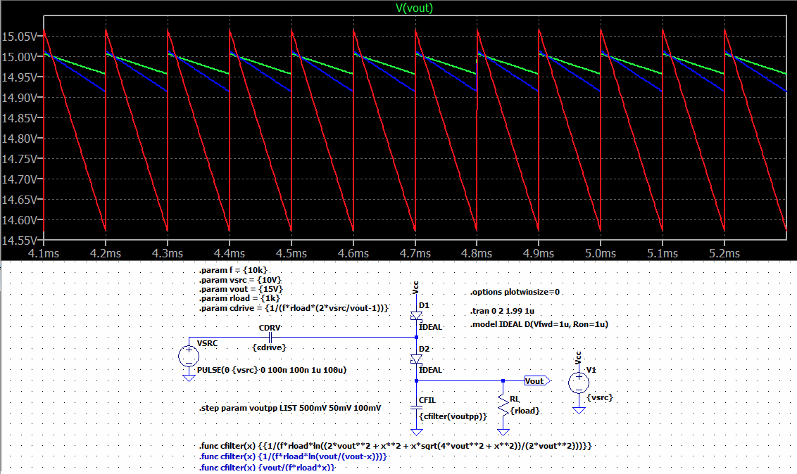
I can, on the other hand, remove much of the kink by instead making the duty cycle very small. For example, say 1%, and with a more gentle transition. In this case, the peak voltage is set by the drive capacitor's formula and the filter capacitor formula more accurately predicts the ripple, as well.
I'll show the same two runs as before. But with new clocking that greatly shortens the discharge duration. First the \$19\:\text{V}\$ output case and second will be the \$15\:\text{V}\$ output case:
\$19\:\text{V}\$:

\$15\:\text{V}\$:

Now, the drive capacitor calculation more closely sets the peak voltage instead of the average and the kink is essentially gone, now.
The advantage here now goes to showing that the filter capacitor design equation very accurately predicts the peak-to-peak ripple. (It did so less well, earlier, because of the fact that the drive capacitor continued to supply charge for half the cycle.)
Between these two pairings of runs (total of four charts), one can see that both the drive capacitor and filter capacitor equations, developed from idealized assumptions, do work well at making predictions -- within the limits of the assumptions used to derive them from theory (such as instant discharge at the rising edge.)
We could further improve (complicate) them by taking into account the fact that charge continues to be provided during the period between the rising and falling clock edge, for example. But that's for another day. At least we know we could do it, if we wanted, and how to approach that refinement should it be needed.
Related Ideas
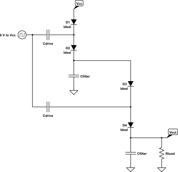
What if you made two of these and arranged them this way:

simulate this circuit
This is just a half-Dickson and it will increase the voltage by another step. So it triples the voltage (about), instead of doubling it. I did this by using the output of the first state as the "\$V_{_\text{CC}}\$" for the second stage. Nothing more than that.
You can continue this idea over and over again.
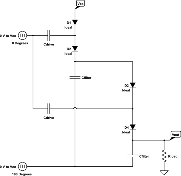
And a full-Dickson would drive the filter capacitors, as well:

simulate this circuit
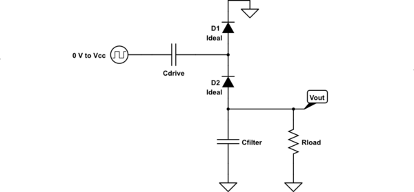
Or you can re-arrange the diodes and get a negative voltage rail this way:

simulate this circuit
All I did was flip the diodes over and instead of \$V_{_\text{CC}}\$ supplying \$D_1\$'s anode, I'm now using ground to supply \$D_1\$'s cathode.
There is an entire family of related ideas here. Be sure to visit the Wikipedia page on voltage multipliers.

