1
\$\begingroup\$

I am trying to design a simple buck converter in LTSpice. Here are my parameters:

Vout = 2.5v
Vin = 5v
Iout = 1A (load resistor will be 2.5ohms)
fsw = 30 kHz
Diode Vf = 0.7
Mosfet switch Rdson = 0.16 ohms

I used the minimum sized inductor and capacitor values from the calculator here: https://www.ti.com/tool/BUCK-CONVCALC.

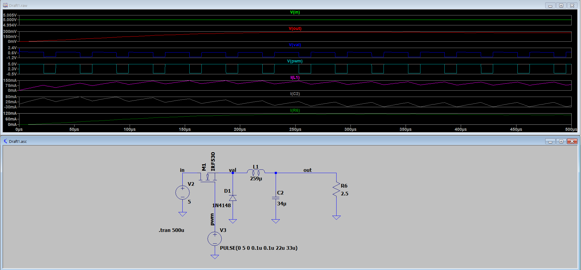
After simulation, I only see Vout = <300mV and Iout (I(R6)) = <120mA. Here are the simulation outputs:

enter image description here

Why is the output voltage and current lower than expected, and how can I fix it?

\$\endgroup\$
1
  • \$\begingroup\$ Do you understand Vgs is too low? \$\endgroup\$
    – D.A.S.
    Commented Apr 17, 2022 at 0:37

3 Answers 3

1
\$\begingroup\$

You have (at least) two significant non-idealities in your circuit.

  1. The N-channel MOSFET needs at least VGS > 3 V to turn on. In your circuit, you only drive the gate to 5 V, so source will only go to about 2 V. At 1 A, it will be even lower. While the 200 V-rated FET is not optimal for your circuit, it can handle 20 V on the gate. If you change V3 to pulse to 10 or 20 V, it will perform better. However, the RDSON is 0.4 Ω, so that will still cause an error of about 0.4 V. The voltage looks like about 1.2 V in your waveforms.

  2. An 1N4148 is a small signal diode and is not rated for 1 A. Even at 1 A, the VF will likely be over 1 V. Your waveform shows nearly 1.2 V.

You are sending in a PWM with about 66 % (22u/33u) duty cycle. The expected output voltage would be 66%*VHIGH + 33%*VLOW. Where VHIGH is the voltage generated by the source of the FET -- say 1.5 V, and VLOW is the VF of the diode (say -1.2 V). Thus you could expect 66%1.2 + 33%(-1.2) = 400 mV which is close to your result.

In addition, the TRISE and TFALL of your PWM are quite slow -- changing these to (say) 0.01 us will improve things.

A full buck converter would use a regulation loop to adjust the PWM duty cycle to achieve the expected output voltage, but your circuit wouldn't be able to achieve more than 1.2 V if you only drive the FET's gate to 5 V -- by driving to 20 V (and/or choosing a device with much better RDSON (and you don't need a 200 V device), you will get a result closer your expected value.

You will also improve things by using a different diode (a Schottky would be best), but lacking that, place (say) 10 1N4148 in parallel. that will reduce the VF significantly.

\$\endgroup\$
0
\$\begingroup\$

You are using an N channel mosfet with a vgs on of 3 to 4 volts. To turn it on you need to supply about 5 volts relative to it's source which means you need a drive voltage of about 10 volts relative to ground.

If instead you use a P channel mosfet then the drive level will be adequate but the gate polarity will need to be reversed.

\$\endgroup\$
0
\$\begingroup\$

The voltage waveforms shown in your simulation for V(Val) suggests that your IRF530 is not turning fully on.

You can check this by raising the gate voltage pulses in your simulation to 10V, to see what happens. If the output voltage corrects itself, then the problem has been isolated.

Indeed, one would expect that the V(Val) would never rise to more than the input voltage minus the MOSFET threshold voltage.

There are various ways to drive a high-side N-channel MOSFET. This video discusses some of the methods available to drive a high-side N-channel MOSFET. An alternative is to use a P-channel MOSFET for your switch (and adjust the duty cycle for the reversed polarity).

You can also improve the situation a bit with a MOSFET with a lower threshold voltage. However, you will still see a voltage drop through the MOSFET when the gate voltage is at the drain voltage. So unless there is some obstacle to one of the various gate driving mechanisms available, or there is an obstacle to using a P-channel MOSFET, I would recommend using one of those two methods.

Reversing the drain and source of the MOSFET runs into the problem that the IRF530, like most common power MOSFETs has an internal body diode connection between source and drain. If connected so that that the source is more positive than the drain, (by one diode voltage drop), the device will conduct, regardless of the voltage on the gate.

\$\endgroup\$

Your Answer

By clicking “Post Your Answer”, you agree to our terms of service and acknowledge you have read our privacy policy.

Not the answer you're looking for? Browse other questions tagged or ask your own question.