4
\$\begingroup\$

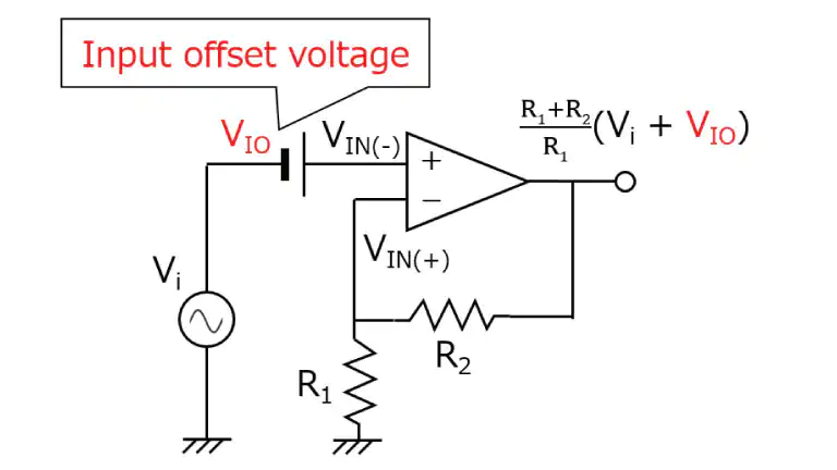
If we have an opamp and we know the input output relation we can obtain a linear function even though there is input offset voltage.

enter image description here

In the above situation as long as we know Vio, and since resistors are fixed we can derive a transfer function between Vin and Vout of the opamp.

What I don't know is whether Vio is a fixed quantity or an unreliable one changing at each power up. I am trying to amplify a DAC output but I am worried about the effect of this offset voltage.

Does it vary with time or supply voltage, or anything else?

\$\endgroup\$
3
  • \$\begingroup\$ good question. You first have to check that on the op-amp's datahseet. does it mention anything like that? (I have never read something like that in any datasheet for example). After that, bear in mind all the factors that determine Voffset (temperature, voltage applied, input voltage ripple, the frequency of the ripple etc etc, they will be mentioned in the datasheet as well). \$\endgroup\$ Commented Apr 28, 2022 at 11:26
  • \$\begingroup\$ Some opamps have ways of trimming the input offset voltage. That would be useless if it wasn't an inherent characteristic of the opamp (and repeatable) So for those opamps you can trim (most of) the offset away on test, and expect the adjustment to remain roughly correct. But expect some variation with temperature, voltage, aging too \$\endgroup\$
    – user16324
    Commented Apr 28, 2022 at 11:30
  • \$\begingroup\$ if Vio is 10mV and it varies +-10mV, it will be between 0 to 20mV. If Vio is trimmed and made zero and still varies +-10mV, it will be between -10 to +10mV. What is the point of trimming it at the beginning? I can understand chopper amplifier but trimming the Vio for a usual opamp doesnt make sense to me. \$\endgroup\$
    – user1245
    Commented Apr 28, 2022 at 11:33

3 Answers 3

7
\$\begingroup\$

In general offset voltage will vary with everything to some degree.

Op-amps that are auto-zero (zero drift) tend to have a relatively low (often negligible) drift with temperature and time (aging) but have other disadvantages.

There are a very few op-amps that do an auto-zero cycle only at power-up which adds an extra element of risk and uncertainty to the power cycling. I would avoid those entirely in pretty much any situation.

None-auto-zero op-amps age to some degree (typically some kind of drift that decreases as time goes on but never really stops) and have Vos changes due to ambient temperature that can be relatively large (say >5uV/°C) or relatively small (perhaps 0.2uV/°C) for the best designs. As always, beware of how the datasheets actually specify drift (it's not a guarantee of the slope over a narrow range, rather, it is typically a 'box' specification over a wide temperature range. Even if you have stable ambient temperature and turn it off for some time, even if the offset voltage does not change with time, there will be a warm-up time while the junction temperature rises to near the steady-state value. If you draw a great deal of current from the output the junction temperature and therefore offset voltage will change as a result of that (you can consider that a kind of low-frequency distortion).

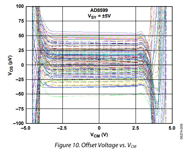
Offset voltage effectively changes with common-mode voltage, which is the CMRR. In particular if they are rail-to-rail input they often have a significant and nonlinear shift in offset voltage with common mode voltage as the two front ends transition. If you can avoid that region, that kind of op-amp can be no worse than a non-RR-input op-amp.

Since those characteristics vary wildly between op-amp designs you need to pick one that meets your detailed requirements. The resistors won't directly affect offset voltage, though they will affect gain drift. If you're concerned with microvolts then you need to consider a lot of other details.

Here is a typical high-precision op-amp (an AD8599) showing Vos change with Vcm, from the relevant datasheet:
enter image description here

And, from the Analog Devices OP07 datasheet, a typical precision amplifier, typical drift with time:

enter image description here

The first hour or day of operation is typically specifically excluded so some burn-in is assumed to get those typical results.

From the LT1028 datasheet:

enter image description here

You can see the (relatively small in this case) warm-up drift, typical aging, drift with temperature. Keep in mind that the actual numbers shown in this datasheet are for one of the very best of breed product and a jellybean op-amp may be orders of magnitude worse.

Changes in bias current will also affect the output offset voltage of your circuit.

Non-precision non-auto-zero op-amps will behave similarly to the above, but often much, much worse. They just don't bother providing the figures because they assume you don't care about 100uV or a few mV here and there.

In conclusion, other than the rare exception I mentioned in the second paragraph above, offset voltage will typically return to the previous value very closely following a power cycle (after a suitable warm-up time has elapsed).

\$\endgroup\$
1
  • 1
    \$\begingroup\$ I couldn't have put it better myself. \$\endgroup\$
    – Andy aka
    Commented Apr 28, 2022 at 13:07
2
\$\begingroup\$

TL;DR: In op-amps not designed as “zero-drift”, the temperature of the die has the most noticeable effect on the offset voltage, everything else being constant.

What I don't know is whether Vio is a fixed quantity or an unreliable one changing at each power up

The power-ups by themselves don’t affect it per se. But everything else does, to an extent that depends on the type of the op-amp in use:

  • open- vs. closed-loop operation,
  • temperature of the op-amp,
  • power dissipation - self heating changes the temperature of the die,
  • input common mode voltage,
  • input bias and offset currents converted into voltages by the impedances of the external components connected to the inputs,
  • power supply voltage,
  • mechanical stress, including thermally induced stress,
  • age of the op-amp (number of hours it has been powered on),
  • output current, when the power dissipation is held constant.

The above list is not exhaustive, but covers most significant contributions. The order of the contributions very is roughly in the most- to least-significant, although this can vary a lot between op-amp types.

Running the op-amp in a comparator application circuit can vastly degrade its effective input offset voltage. The offset voltage is specified assuming a closed loop operation. The effective comparator-mode offset voltage can differ, depending on the design of the op-amp. It can also vary a lot depending on the slew rate of the input differential voltage, due to internal circuits acting as differentiators. Typically, most precision is obtained from dedicated comparators: op-amps are a poor man’s comparators.

In op-amps that don’t have offset zeroing, the temperature has the most noticeable short-term effect. The common mode voltage can also have significant effects that present as nonlinearities. To minimize the common mode influence, the power supply rails need to be bootstrapped to the common mode voltage. Inverting configuration has a constant common mode voltage and thus is inherently devoid of this contribution. The power supply voltage, mechanical stresses and aging are further contributors.

In the most demanding precision applications, the power-ups themselves may introduce a thermal stress cycle that contributes a very small offset voltage change each time it occurs. This effect tends to “anneal” with each power cycle, and eventually it reaches some steady state. This highly depends on the op-amp’s design, packaging, mounting, PCB substrate, etc. These effects become important when designing, say, 7+ digit voltmeters - they are dwarfed by other effects in lesser accuracy uses.

\$\endgroup\$
1
\$\begingroup\$

Note that the input voltage offset (due to input circuit imbalance), which for a specific physical device (a single one) varies mostly with temperature, is only one of the non-ideal characteristics that are modeled as an input voltage at the input pins.

Does it vary with time or supply voltage etc?

Power supply rejection ratio can also be modeled as a variable input voltage offset, so yes (indirectly).

Common mode voltage gain is another example, as well as imbalance caused by offset current through large input resistances (even the polarity may change close to the rails).

For a specific model all these contributions add to the equation shown in the question, but they may differ by an order of magnitude or more. Which means that, without significant temperature variation, a software compensation (or even an external imbalance compensation with resistors) may be enough for the application requirements.

Thanks to @SpehroPefhany's contribution I can provide a graphical representation of what I mean about how two sources of voltage offset can be relatively compared:

enter image description here

\$\endgroup\$
5
  • \$\begingroup\$ external imbalance compensation would not help if Vio varies rgiht? Vio can be zero or 10mV but if it varies variation will be the same isnt it? I mean specifically for my question the variation will be the same in case of a temperature drift correct? Since I can obtain transfer function Im not trying to zero the Vio. Because if Vio made zero it will again vary same way. I hope I made my question more clear. \$\endgroup\$
    – user1245
    Commented Apr 28, 2022 at 11:24
  • \$\begingroup\$ And what do you mean by software compensation? \$\endgroup\$
    – user1245
    Commented Apr 28, 2022 at 11:25
  • \$\begingroup\$ For errors due to common mode, isnt it better to fix the reference voltage or ground to non inverting input and apply the signal to inverting input? Applying Vin to non inverting input will vary the common mode error proportional to Vin(?) \$\endgroup\$
    – user1245
    Commented Apr 28, 2022 at 11:27
  • \$\begingroup\$ " what do you mean by software compensation?" Since you mentioned a DAC I assumed you could calibrate and adjust the software for each device if, and only if, all the conditions I mentioned are present to make the compensation (software or hardware) possible and effective. \$\endgroup\$
    – devnull
    Commented Apr 28, 2022 at 11:31
  • \$\begingroup\$ "isnt it better to fix the reference voltage" It is not about the accuracy of the full scale, but the output range. "ground to non inverting input and apply the signal to inverting input" Sure, this circuit topology practically eliminates the common mode voltage problem. \$\endgroup\$
    – devnull
    Commented Apr 28, 2022 at 11:33

Your Answer

By clicking “Post Your Answer”, you agree to our terms of service and acknowledge you have read our privacy policy.

Not the answer you're looking for? Browse other questions tagged or ask your own question.