I'm new to Altium and want to measure distance between two pads' solder-mask clearance using Reports-->Measure. I tried activating solder-mask layer only and then tried to measure like regular measurement method but snap was never picking the solder-mask edge. I need to measure this distance often in order to know the solder-mask clearance between pads in parts where there seems less spacing or less pitch.
4 Answers
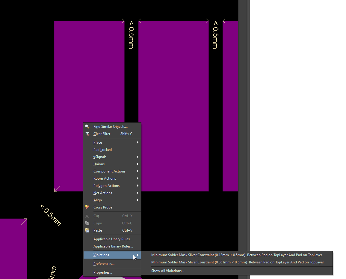
Another non-ideal approach is to set the design rule for solder mask sliver to something large such as 0.5mm and then run design rule check.
Right click on an offending pad will give you Altium's take on the spacing.
Of course you have to remember to reset the design rule to the lower value.
-
\$\begingroup\$ Thanks for this workaround but it won't solve my purpose may be, because i have that type of pads and parts where measuring is necessary. and moreover RF parts are being created. Thanks for you lovely images to depict your answer, really appreciate it. Now I am sure that this is limitation of Altium itself. \$\endgroup\$ Commented May 4, 2022 at 13:37
Altium Designer doesn't snap to the soldermask layer, even if it's the active or only shown layer. The best you can do is zoom in quite a bit and hold Ctrl while placing the measuring points to get as close as you can.
Aside from that you can get the exact amount by doing the following:
- Measure the distance (d) between the two pads' center points.
- Subtract the pad height or width (w) (whichever is applicable to your measurement axis).
- Subtract the soldermask expansion (e) amount multiplied by 2.
Gap between soldermask expansion openings: $$d-w-e2$$
For example, in my image, the pads are 0.5 mm apart vertically. Pad height is 0.25 mm. The soldermask expansion amount is 0.102 mm.
$$0.5 - 0.25 - (2\times0.102) = 0.046$$
As you can see, my measurement using the first technique was off by 0.003 mm.
-
\$\begingroup\$ Your first method might give somewhat near results but doing calculations all the time would be a hectic task. Though I know that same can be calculated using subtraction but again you cannot apply this calculation method at corner pins in case of QFN to check whether enough mask clearance is there or do we need to do chamfer the corner to have proper SM-clearance. Thanks for your detailed reply, I really appreciate it. \$\endgroup\$ Commented May 4, 2022 at 13:32
Unfortunately, Altium doesn't allow primitive measurements on the solder mask layer.
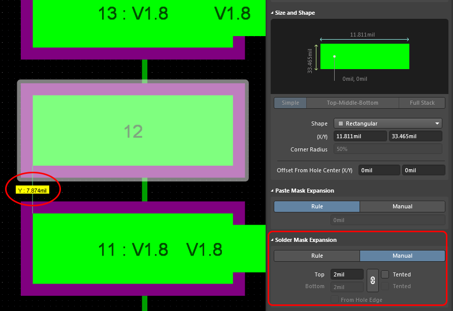
Make the pad layer (top or bottom) active and measure the gap between pads using Reports -> Measure Primitives.
Click on the pad to bring up the pad properties where you can determine the solder mask expansion dimension.
Subtract 2*(Solder Mask Expansion) from the gap between the pads.
In the example below, the gap between pads is 7.874mil and the solder mask expansion is 2mil. Thus, the solder mask gap is \$ 7.874mil - 2*2mil = 3.874mil \$, alas, less than ideal.
-
\$\begingroup\$ Thanks for your reply, well this can certainly be applied where measurement is straight but can same me measured at corner pins in the case of QFN or have different shape of soldermask. I believe, Altium shall give this function in order to avoid in last moment changes if FDM report is being received from CMs. Thanks \$\endgroup\$ Commented May 4, 2022 at 13:26
Another ugly approach which works with a lot of tools is:
- use an empty layer
- use a circle tool with the minimum distance as diameter
- try to place circles where the distance is needed
If you can't manage to fit a circle in there, the distance is too small.
Benefit: can be used to document the spacings
Con: not very precise, fiddly, time consuming.


