I'm trying to implement an inverting Cuk DC-DC converter on a 2 layers PCB, in order to generate a -3.3V rail from 3.3V, but the circuit affects greatly the input rail. The 2 rails are used to power 4 Op Amps. I'm using the LTC1617 from Linear Technology and I copied the circuit from the datasheet, modifying the components values to fit my needs.
The schematic is the following:

I simulated the circuit in LTSPice and everything seems to work.
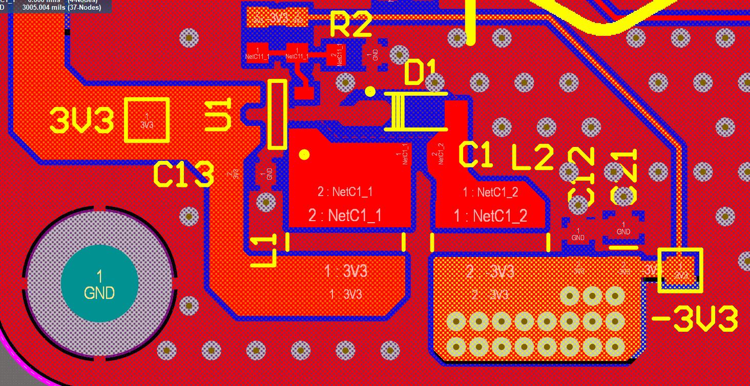
I had to implement the design on a 2 layers board, and I followed the suggested PCB layout that can be found in this application note:

my layout:
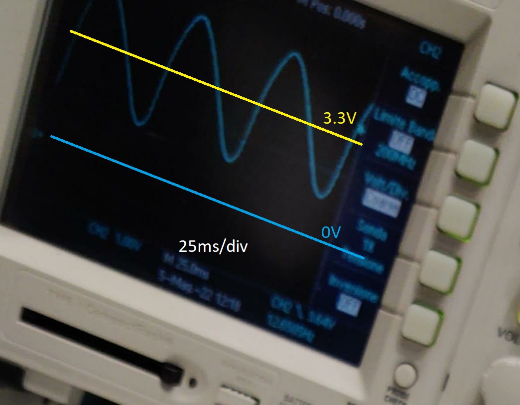
When I power the circuit, the output voltage is exaclty as in the simulations (stable -3.3V with 20mV ripple) but the 3.3V input gets greatly affected. The voltage supplied from a bench power supply becomes a large smoothed sawthoot wave, with a pk-pk value of 5V, mean value of 3.3V and frequency 10Hz.
Picture from the scope (sorry if it's not quite readable, but it's the only picture I took):

It seems to me that somehow the switching voltage at the SW pin node pass through the inductor and present itself at the input pin. I also can't explain the very low frequency. From the simulations the voltage on the SW pin reaches exactly the same voltage values as the ones that I find at the input:

This is the first design I make with a DC-DC converter and I'm not really acquainted with DC-DC converter topologies so I'm not sure where to look for errors. I'd greatly appreciate suggestions on how to debug the circuit. Thanks a lot.
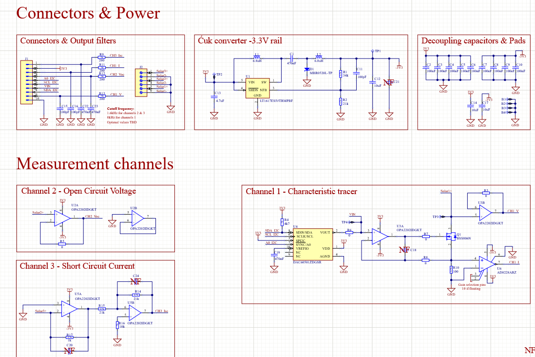
I'm also attaching a picture of the full schematic (the DAC is not soldered on the board):


