4
\$\begingroup\$

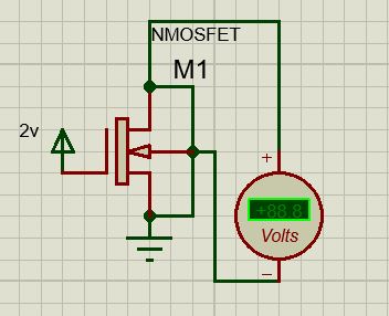
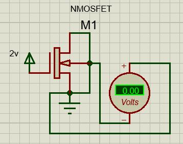
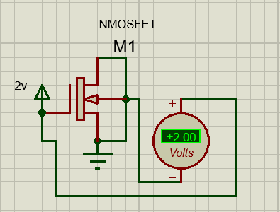
Let us assume that an NMOSFET has its source, drain and substrate grounded therefore VDS and VSB=0 V . We apply a gate voltage VGS=2 V and I want to know how this potential is distributed as we move from gate towards substrate.

Let us assume the threshold voltage to be VT=0.7 V. Now I know that since the MOSFET is in inversion, a charge density Qinv= Cox*(VGS - VT) will appear in the inversion layer. The threshold voltage will be divided into two parts:

  1. Change in surface potential from φS to -2φf where φf is the bulk fermi potential.
  2. To support the depletion region charge due to increased depletion region width at inversion.

Let us assume that VT is equally divided between these two components and assign 0.35 V to both. Now I believe that potential at the surface under the gate must be atleast at 0.35 V because we still need to account for bending of band and change of surface potential but since the MOSFET is under inversion, an inversion layer links the surface, drain and source and therefore they must be at 0 V (since we assumed they are grounded). So where am I going wrong?

Edit: https://demonstrations.wolfram.com/AppliedVoltageOnAnIdealMOSCapacitor/

This demonstration simulates the effect of an external bias on a MOS capacitor. I checked the graph of electrostatic potential as I increased the gate voltage and I found that VSurface increases indicating that some part of applied voltage is used to increase the surface potential to cause inversion. There is a potential difference between surface and substrate. But since in MOSFET we have grounded source, drain and substrate to 0 V and source, drain and surface are connected through an inversion layer in inversion mode, we have set VSurface to be at 0 V. So there is no potential difference between surface and substrate. Then how can we achieve inversion?

\$\endgroup\$

4 Answers 4

2
\$\begingroup\$

The potential throughout the channel will be the same as S and D (i.e. 0).

This is because that is a continuous conduction region with no current flowing.

The potential across the GOX will be VG.

There is a slight twist to this - if you define '0V' as the V at the external S terminal, then due to work function difference, the actual V will be non zero, but this is not observable.

An excellent book on this is 'Operation and Modeling of the MOS Transistor' by Tsvidis and McAndrew

\$\endgroup\$
3
  • \$\begingroup\$ I have edited my question to add some more details can you please look at it again? \$\endgroup\$ Commented Jun 5, 2022 at 6:25
  • \$\begingroup\$ I understand the potential due to work function will be non zero at the source and it's non observable. But I am talking about situation where I have applied gate voltage, some part of that voltage will increase the surface potential to cause inversion, but since the gate drain surface are all connected through inversion layer, it seems surface potential will be at 0 V too. I am unable to understand how can surface be at non zero potential and at zero potential at the same time. \$\endgroup\$ Commented Jun 6, 2022 at 18:24
  • \$\begingroup\$ Also the link I have shared in my edited answer also proves the fact that when gate voltage is increased, surface potential also increases. The problem is how to explain this in MOSFET with source drain and substrate grounded. \$\endgroup\$ Commented Jun 6, 2022 at 18:26
0
\$\begingroup\$

Potential at the Gate Potential at the Drain Potential at the source

Potential through the drain and source will be zero.

\$\endgroup\$
2
  • \$\begingroup\$ The Original Poster (OP) mentioned in “Let us assume that VT… So where am I going wrong?“. That seems to be the main point in OP’s question. Consider writing a few line added to your answer to make the context of how it answers the question. \$\endgroup\$
    – EJE
    Commented Jun 5, 2022 at 13:16
  • 1
    \$\begingroup\$ I'm not sure this answers the question, because they seem to be wanting to know something about the underlying physics that aren't modelled in SPICE simulators. An FEM simulation would be more helpful, I suspect. \$\endgroup\$
    – Hearth
    Commented Jun 5, 2022 at 16:35
0
+50
\$\begingroup\$

My understanding is that most of the surface potential is dropped across the oxide portion under the gate, with D/S/B tied to ground. This seems consistent with your comments.

Sources.

  1. "In inversion and accumulation , the vast majority of the gate voltage is dropped across the oxide

In inversion, the depletion width remains ~ constant Thus, φS can not be much less (greater) than 0 for p-type (n-type)

Thus, φS can not be much greater (less) than 2φF for p-type (n-type)"

2)"We take N-channel MOSFET as an example to analyze the capacitance with the source/drain connected to the bottom (substrate). The capacitor composition between the gate and bottom is shown in Fig. 1(b), where the red line is electrically connected. enter image description here

If the gate voltage is smaller than a threshold voltage Vth, the total capacitor still performs like a MOS CAP because an inversion layer is not yet formed to short-circuit the depletion region. However, when the bias voltage becomes larger than Vth, the formed inversion layer, source, drain, and bottom are connected as one terminal to shortcircuit all the capacitors among them. After that, only the oxide capacitance is left since one of its terminals is the gate. The total capacitor between the gate and bottom quickly increases from Cdep to Cox, which is the total oxide capacitor. The deviation is usually more significant than 50% as shown in Fig. 1(c), because Cox is larger than Cdep."

\$\endgroup\$
2
  • \$\begingroup\$ Yes I agree that most of the potential drops across oxide but still a non zero voltage does exist as surface potential. For a p type doping of 10^16 cm^-3 in Si makes surface potential to be approximately 0.3486 V at threshold voltage. I don't think it increases much after inversion but still it's significant enough so as not to be rounded to zero. And I just can't find any source where this is explained. \$\endgroup\$ Commented Jun 7, 2022 at 21:52
  • \$\begingroup\$ And yes I do understand that the surface potential of 0.3486 V has contribution from both the gate voltage and the work function difference. \$\endgroup\$ Commented Jun 7, 2022 at 22:03
0
\$\begingroup\$

The above explanation is very clear in terms of vertical potential. One quick note when you go from source to drain just under the oxide (channel of Silicon), is the VDS is mainly drops across depletion region of pinch-of or depletion region between drain and body or depletion region between source and body. They actually act as a capacitor, C_body/drain and C_body/source. So, I think if you think it that way, you would be able to see the channel under the oxide with phi_s coming from VG.

\$\endgroup\$

Your Answer

By clicking “Post Your Answer”, you agree to our terms of service and acknowledge you have read our privacy policy.

Not the answer you're looking for? Browse other questions tagged or ask your own question.