Design Requirements:
The purpose is a linear DC power supply for 12-volt aircraft, marine, and amateur radio equipment
- power source 20 volts @ +/-10%. (output 85W = 6A*14.2V)
- Rser on V1 = 0.4 or just say Output Voltage = 14 volts as shown
- adjustable 10 to 15V via R5/R6 with pot.
- Tested and works Output Current = 6-amps.
- Tested and works Current Limit not shown. Have a working model.
- Line/Load Regulation: 14 VDC @ 0 to 5-Amps = <0.1% ( Model exceeds spec.)
- Ripple and Noise <200 uVpp
- Load Step Response 0 to 4 to 0-amps: better than +/- 200mv recovering in 10 us. This is the one I am having trouble with.
I need a mentor to help me put the finishing touches on a 14-volt 5-amp DC power supply. I am an EE, RF engineer, ham radio operator, and first-time LTSpice user. It has been 30 years since I last worked on discrete components.
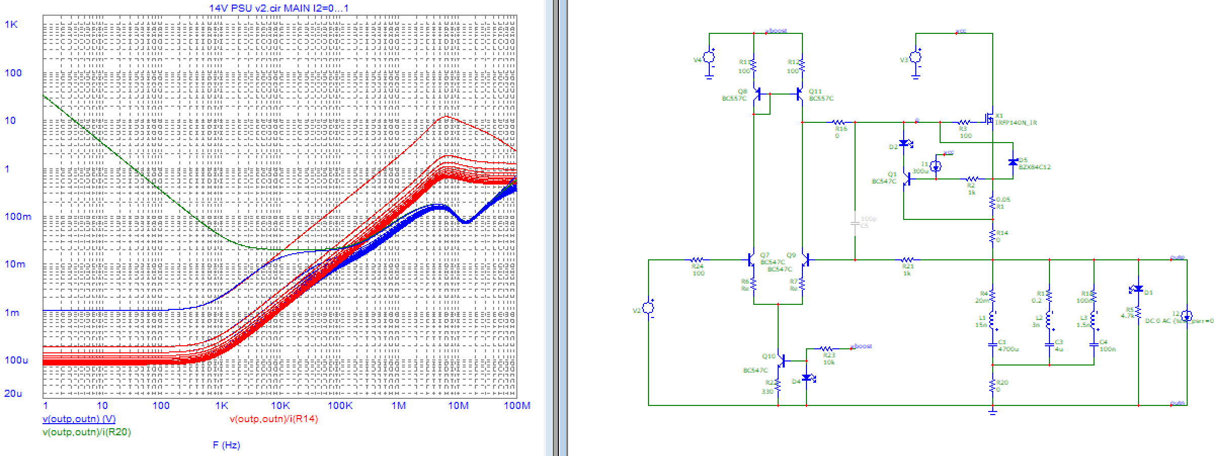
I did some homework, looked at some designs I liked, and came up with the circuit below. It worked great on LTSpice until I added the second test circuit on the right. I am sure the circuit design needs some Compensation somewhere, or perhaps a different op-amp, but I am lost.
Brief description of the circuit. It is a Floating Ground voltage regulator. U1, C1, C2, R1, and R2 create a soft-start -5-volt voltage reference applied to U2 inverting input. R5 and R6 provide feedback to the op-amp non-inverting input.
D1 is an OR gate on the op-amp output to allow a current control circuit (not shown) to integrate into the control loop. As load current increases, the regulator drive voltage increases to compensate. At the same time, the current control voltage falls lower as the load current increases to a point where it takes control of the loop. R4 is a 10K pull-up resistor that guarantees M1 will start and force U2 to sink current discharging gate capacitance on M1. R3 is a 100-ohm gate resistor, which helps with compensation according to manufacturing data.
M1 is the pass element capable of supplying 10-amps of current. Or can be reconfigured to drive multiple parallel NPN transistors for higher output currents. C3 is a 4700ufd filter connected across the output. R7 is a bleeder resistor that doubles as a load resistor in LTSpice and output voltage monitor.
M2, V2, R8, and R9 are test circuits turning on/off a 4-amp load to test the output response and why I am here. Not happy with what I am seeing. The trouble starts when I connect the test circuit and configure V2 as a PULSE circuit—configured as a Sine Wave generator with 7-volt DC bias, 4 volt 1000 Hz signal performs as expected, and the output voltage is a flat line. The output signal from the op-amp is a pretty sinewave, as is the output current seen in R8 with a magnitude of 4 amps...
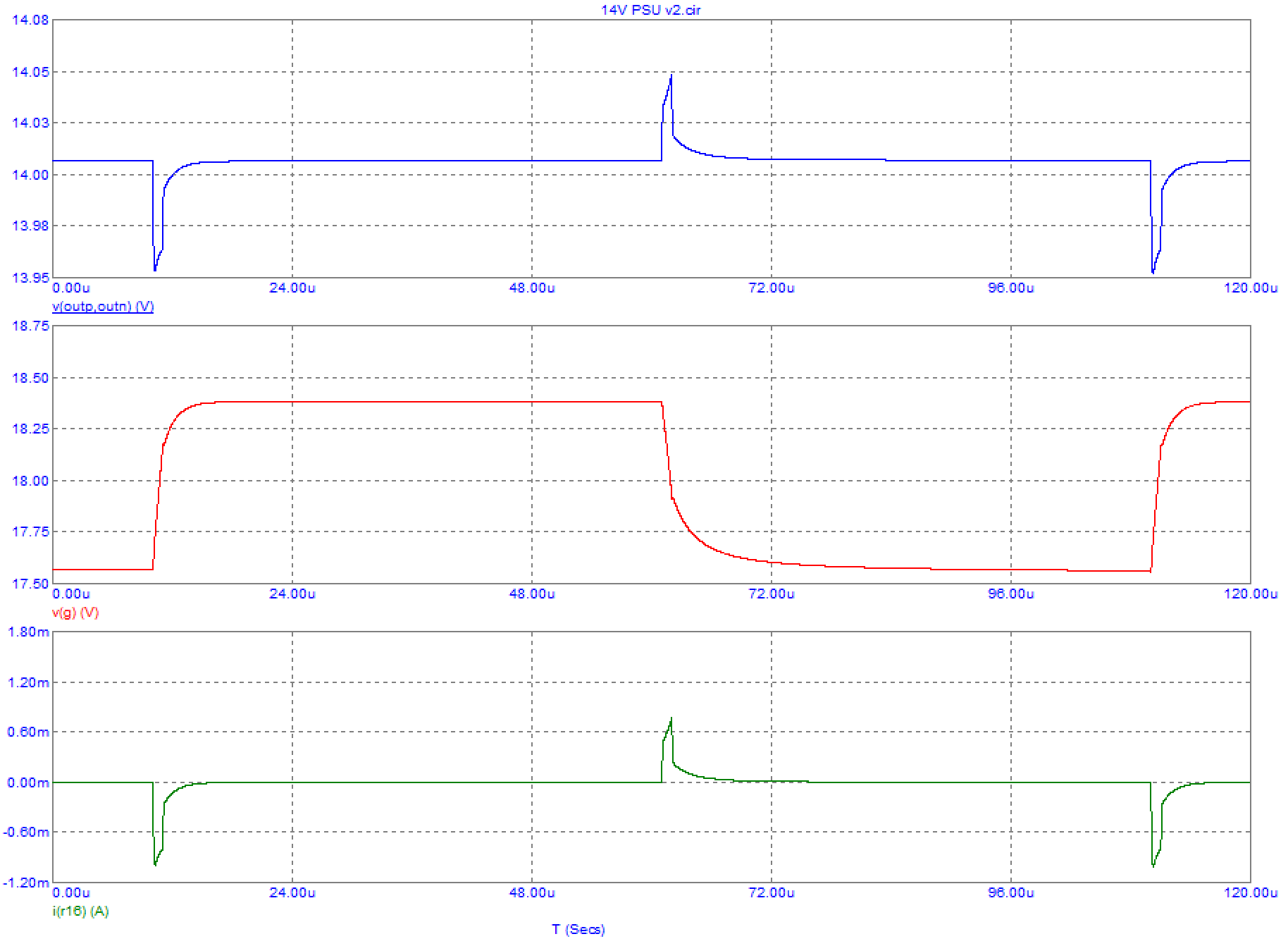
Configure V2 as a Pulse Generator as shown, and things get ugly depending on how fast/slow I set the rise and fall times. At 1us and faster rise/fall times, note the voltage spikes across the output represented by the current in the IR7 trace. It dips to 13.88 volts and peaks at 14.1 volts.
The second trace is the op-amp's output voltage measured at the gate of M1. I expect it to look like a nice squarewave but see that nasty falling edge spike. I suspect a result of gate capacitance but am clueless about how to fix it. Increase rise/fall times, and things improve. At 10us, results look acceptable. At 100us looks excellent.
Can someone help me out? Appreciate all comments, suggestions, and answers.
THX


