Showing the forest behind the trees
I keep wondering how it is possible to analyze a circuit without recognizing and showing its main building blocks and the principles they implement... especially when it comes to such a famous circuit solution… Because we are humans, not computers... and we need that…
Redrawing the circuit
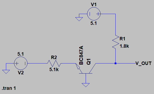
Let's start doing it by first redrawing the circuit in a way that would remind us of something known:

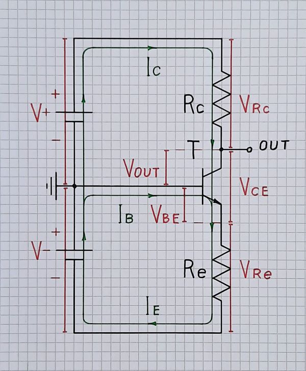
First, we can combine the two power supplies (positive and negative) into one common split power supply by connecting them in series and in the same direction. We see that the total voltage of this composite source is equal to the sum of the two supply voltages. Their midpoint serves as ground and as a zero voltage input source. We draw the positive voltage source above and the negative voltage source below the zero voltage line.
Then, we can draw the transistor with the collector and the collector resistor at the top... and with the emitter and the emitter resistor at the bottom... and turn the base to the left (because this is the input).
We can also visualize the circuit voltages and voltage drops by vertical voltage bars (in red) with proportional height (in association with a water column). Thus we can visually compare their values and polarities. We draw the positive voltage bars above and the negative bars below the zero voltage line.
Finally, we can visualize the current paths and directions by current loops (in green). Thus we can see an interesting fact - the base current is entirely provided by the negative power supply.
Emitter degeneration
From the redrawn circuit we can easily recognize the common-emitter transistor amplifier stage with series negative feedback in the emitter. This configuration was initially invented in tube circuits (cathode degeneration) and later in transistor circuits (emitter degeneration). We can present this circuit in three steps:
Emitter follower. The role of the transistor T is to copy the input voltage V- across the emitter resistor. For this purpose, it compares V- and Ve by subtracting them in series and adjusts its collector current to make Ve equal to V- (with a small error of Vbe). Referenced to the middle point (ground), this means that the transistor creates a copy of the ground at its emitter (aka virtual ground).
Current source. Keeping up a constant voltage across a constant resistor, the transistor acts as a constant current source.
Voltage amplifier. This current "creates" a voltage drop across the collector resistor... and we use its complement to V+ as an output voltage.
"Voltage divider"
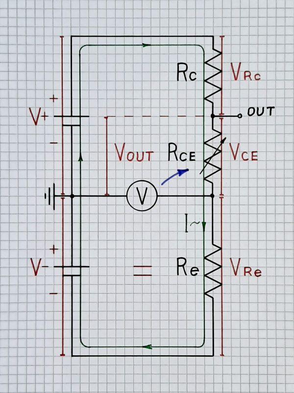
Of course, we can consider the two constant resistors Re and Rc in series as a kind of voltage divider athough it is a little strange. The collector-emitter part of the transistor can be considered as a varying "resistor" Rce.

Imagine we vary Rce and observe the sensitive voltmeter V (zero indicator) so that to keep its reading equal to zero. Thus we play the role of the transistor in this "negative-feedback game". The current flowing through Re and Rc is the same; so VRc/VRe = Rc/Re Figuratively speaking, the current like an "electrical transmission" connects the two voltage drops.
It is interesting that this "voltage divider" can act not only as an attenuator (when Rc < Re) but also as a follower (Rc = Re) and amplifier (Rc > Re).
Another interesting feature is that this voltage "divider" is inverting (because we use the complementary voltage as an output). We can even use both emitter and collector voltages (as in the so-called "phase splitter").

