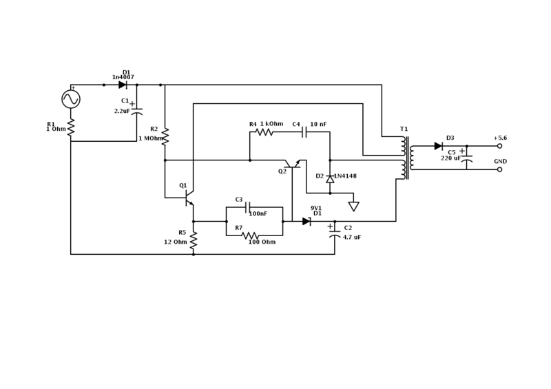
I have an old Nokia phone charger with 5.6 V output, so I tried to adjust it to 12 V. By changing the Zener diode though I manged to do that, but I can't understand its circuit (I replaced the 9v1 with 16v Zener). I would really appreciate any help to understand it. I already understand most of the circuit, but the feedback and switching action isn't clear.
-
2\$\begingroup\$ "I cannot understand this circuit" -- most of which is not isolated from line voltage! \$\endgroup\$– KazCommented Mar 25, 2013 at 6:21
-
\$\begingroup\$ i think Q1 with the upper winding and R5 manage the switching action of the half rectified ac voltage (by D1 and C1). Q2 with the lower winding sense the voltage as when the D1 break conducting current to Q2 base which in turn will open conducting current away from Q1 base so as to turning it off. but what i miss what the remaining components do(C3,R7,C2,R4,C4,D2) \$\endgroup\$– Mostfa MahmoudCommented Mar 25, 2013 at 7:56
-
\$\begingroup\$ I'm sorry but i cant figure why it isn't isolated from line voltage i think it is isolated by the means of T1. and thank you for your time. \$\endgroup\$– Mostfa MahmoudCommented Mar 25, 2013 at 8:11
-
\$\begingroup\$ According to the schematic, the secondary winding of T1, diode D3 and capacitor C5 are isolated. The rest of the circuit isn't. \$\endgroup\$– KazCommented Mar 25, 2013 at 8:18
-
\$\begingroup\$ i think because it is a cheap small power supply so it was more cost efficient to isolate the output circuit only not the switching circuit . however isolation isn't my concern now as i seek understanding the switching action \$\endgroup\$– Mostfa MahmoudCommented Mar 25, 2013 at 8:36
1 Answer
The top left winding of the transformer is the primary power input. It is controlled by Q1 which can switch the half-wave rectified AC power across this winding. A certain amount of current limiting is provided by R5.
R5 also is used by Q2 to turn Q1 off as the current through R5 reaches a certain point. It detects the emitter voltage on Q1 via R7 and C3.
The bottom left winding of the transformer controls the output voltage of the switcher - it also turns Q1 off (via Q2) when a certain DC voltage is reached and this is governed by the zener diode.
R2 is there to allow the circuit to "start-up" and it provides bias for Q1.
The output winding runs open-loop but if the transformer is reasonably well-coupled on it's windings it will provide a half-decent regulated output.
I think R4 and C4 are to control the switching frequency of the thing but maybe someone else can offer a thought or two on this?
-
\$\begingroup\$ thank you very much for lighting things up for me. but what is C2 there for . and why C3 with R7 isn't R7 sufficient. \$\endgroup\$ Commented Mar 25, 2013 at 15:31
-
\$\begingroup\$ @MostfaMahmod there is an anomaly with the circuit diagram that makes it difficult to interpret and particularly around C2. Note that diode D2 shows it connected to a ground symbol and also note that this ground symbol isn't used elsewhere - i'm assuming therefore that C2 smooths the voltage coming from the bottom left hand coil after being rectified by D2. R7 may not be sufficient and possibly, without C2 Q1 and Q2 together may find a quiescent equilibrium half-conducting and half not; neither performing any bang-bang switching and of course this is no good! C2 might keep things unstable!! \$\endgroup\$– Andy akaCommented Mar 25, 2013 at 19:08
-
\$\begingroup\$ i agree with you that the diagram isn't well drawn (I'm not good at drawing schematics) but thank you for your note i will take it in consideration next time :) . \$\endgroup\$ Commented Mar 26, 2013 at 5:37