1
\$\begingroup\$

I'm trying to understand how a voltage doubler using a switched capacitor circuit affects the charge being distributed from the input to the output.
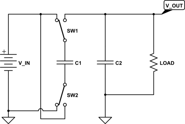
schematic

simulate this circuit – Schematic created using CircuitLab

The circuit operates so that during first phase \$V_{IN}\$ is charging the capacitor \$C_{1}\$ and during second phase the \$C_{1}\$ is connected in series and between \$V_{IN}\$ and \$V_{OUT}\$ and the voltage is doubled. However, theoretically, the maximum output current gets halved.

Now, if current is really halved, does this mean that the charge initially transferred to \$C_{1}\$ halves too (since this relation applies \$Q = I*t\$), or does it stay that same and the time needed to distribute the charge from \$C_{1}\$ to load doubles at the halved current?

P.S.: This might seem a bit weird question but I'm really eager to know the actual answer to this. Also, this has something to do with designing a circuit for charge transfer between battery cells. That is why I'm interested what happens to the amount of charge transferred over to load.

\$\endgroup\$
17
  • 1
    \$\begingroup\$ @Jens Are the high current switching transients the only problem when compared to inductor counterpart for cell balancing? Some research has been put into reducing such transients: ieeexplore.ieee.org/document/4443901 \$\endgroup\$
    – lucenzo97
    Commented Jun 12, 2022 at 8:58
  • 1
    \$\begingroup\$ @Keno I think I may cover how to approach an analysis in this prior response on EESE. +1 on the question! \$\endgroup\$
    – jonk
    Commented Jun 12, 2022 at 16:28
  • 1
    \$\begingroup\$ @Keno Unless you use several MHz switching frequency you need electrolytic capacitors of high quality and even these degrade sooner or later. Good conducting switches are a problem here as well. The signal preparation for 4 FET can be a hassle for multiple cell chains. If you just want to compensate different cell leakage currents, an unregulated voltage double charge pump chip will work. \$\endgroup\$
    – Jens
    Commented Jun 12, 2022 at 16:44
  • 1
    \$\begingroup\$ @jonk I will surely go through each section of your answer, as I assume (from previous experiences) that you provided with quality content :) \$\endgroup\$
    – lucenzo97
    Commented Jun 13, 2022 at 10:04
  • 1
    \$\begingroup\$ @Keno Sounds to me as though Jens has specific, expert knowledge on the topic and would be able to write up an excellent answer. I could write, but it would feel like copying what I wrote before. If you find something that is still missing when reading that answer, feel free to mention it. Or if you need an LTspice simulation that demonstrates what I wrote delivers quantitative prediction, using ideal switches rather than ideal diodes, that also can be easily shown. \$\endgroup\$
    – jonk
    Commented Jun 13, 2022 at 16:55

1 Answer 1

4
\$\begingroup\$

When C1 is switched across V_IN, it consumes current (charge) as it (re)charges.

When C1 switches in series with V_IN (thus doubling it), it also consumes current from V_IN as it (dis)charges and replenishes the load.

Note that current is consumed from V_IN in both states, but (new) charge is delivered to the output only in the 2nd state -- this is the origin of the current halving -- consider that roughly equal currents are consumed in each stage from the input, but only on the 2nd state is current delivered to C2.

\$\endgroup\$

Your Answer

By clicking “Post Your Answer”, you agree to our terms of service and acknowledge you have read our privacy policy.

Not the answer you're looking for? Browse other questions tagged or ask your own question.