I suspect I am making a probe connection mistake, but couldn't figure it out.
The circuit works fine in LTSpice but I don't get anything in a real experiment.
What might be the problem?
I suspect I am making a probe connection mistake, but couldn't figure it out.
The circuit works fine in LTSpice but I don't get anything in a real experiment.
What might be the problem?
As @horta suggested, use wires when needed and "see" the "dot" connection.
You should see something like this (distorted.)
If oscillation does not start (R3 < = 21k,) make this resistor a little greater as also @WhatRoughBeast suggested in his comment.
If you want something more "sinusoidal", you should use diodes as a gain "limiter".
Here is an example.
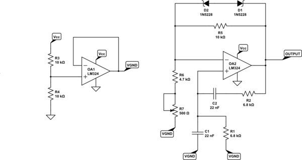
I may as well add a practical circuit using cheap parts.
The LM324 provides roughly four LM741's in a single package. (Nice, if you consider having an LM741 nice.) At least the "knock-off" ICs are cheap (around 5 cents each, if you look around a bit and are willing to buy 100 of them -- and you are willing to risk the fact that their performance won't be anything like a real LM741.) And they can be used with a single rail, too, if you construct a "virtual ground" for them. (Shown in the schematic below.) Since there are a bunch (four) opamps in an IC package, this is also cheap and easy to do. This can save you the difficulties related to creating a bipolar supply. (Note: Although I still do have some LM324's from many decades ago, I haven't used one in about the same period of time -- decades.)

simulate this circuit – Schematic created using CircuitLab
That uses half an LM324 IC. The potentiometer is needed so that you can dial in oscillation. If \$R_7\$ is too small, you will get oscillation but with distortion. If \$R_7\$ is too large, you won't get any oscillation and the output will just settle on some DC value. Having the potentiometer in the circuit means you can build these over and over and make adjustments for the vagaries of parts.
In the above, I am thinking about \$V_{_\text{CC}}\ge 9\:\text{V}\$, or so. That supply rail simulates as:
Here's the FFT:
freq: 1/(t2-t1)=1050.42

Harmonic    Frequency    Fourier    Normalized   Phase      Normalized
 Number       [Hz]      Component    Component  [degree]    Phase [deg]
    1       1.050e+03   3.090e+00   1.000e+00    -107.87°       0.00°
    2       2.101e+03   7.771e-04   2.515e-04     176.48°     284.36°
    3       3.151e+03   3.885e-02   1.257e-02     -12.03°      95.84°
    4       4.202e+03   2.015e-04   6.522e-05    -119.87°     -12.00°
    5       5.252e+03   4.612e-03   1.492e-03     -24.53°      83.34°
    6       6.303e+03   1.153e-04   3.732e-05    -167.34°     -59.47°
    7       7.353e+03   1.004e-04   3.248e-05      57.14°     165.02°
    8       8.403e+03   1.107e-04   3.583e-05      70.47°     178.34°
    9       9.454e+03   2.440e-04   7.896e-05     114.42°     222.29°
Total Harmonic Distortion: 1.266211%(1.266473%)
If you have a bipolar supply, obviously there is no longer a need for the left-hand section that develops \$V_{_\text{GND}}\$.
If you don't want to include zeners, you can use a multi-feedback amplifier design to get to a similar place -- again with two opamp sections. But I suppose that isn't of interest, so I'll hold short on that topic.
This is a practical circuit. Previously built and tested.
The J-FET provides the automatic gain control.
R8 & R3 linearise the J-FET