0
\$\begingroup\$

I am testing an SPX3819M5-L-3-3 LDO in SOT-23-5 pkg. Its max. Vin is from 2.5 V to 16 V. I need 300 mA, so as a load I connected Vout to a 10 Ω, 10 W resistor to GND.

When I input Vin more than 6 V, the output voltage Vo begins to drop. According to the data sheet spec. table I should get about 0.6 V drop at around 300 mA. According to the charts I should be around 3.3 V.

Vin    Vo                        Io
9 V    drops from 3.3 to 1.8 V    173 mA
8 V    drops from 3.3 to 2 V      200 mA
7 V    drops from 3.3 to 2.6 V    250 mA
6 V    stays at 3.3 V             311 mA

If I cool it with an air can, Vo goes back to 3.3 V. Any ideas why at higher Vin, Vo drops so much?

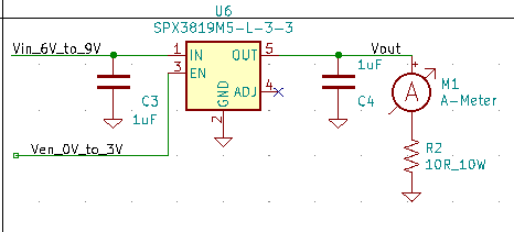
enter image description here

\$\endgroup\$

2 Answers 2

0
\$\begingroup\$

You cannot use a 1W load on 3.3V with 16V input as 300 mW equates into 4.5W with only 1W going into the load. The thermal resistance is given as θja SOT23-5 191°C/W. You can do this with a better supply and if needed a buck regulator even if it is just to drive 3.5V into the LDO if you need low ripple.

\$\endgroup\$
3
  • \$\begingroup\$ How about if i am using only 9V input? I am using lab power supply now, but I was going to use 9V battery as input. So, are you basically saying that i cannot use the LDO w/o a heatsink? Thanks. \$\endgroup\$
    – vgeng
    Commented Jul 5, 2022 at 1:21
  • \$\begingroup\$ 16V? 9? even with a heatsink N.G. Look at the Thermal resistance you would need and compute the temp rise. Then with maybe 4 Wh 9V cell it won't last long . Try a 3.6V battery instead. (LiPo or Li Ion) \$\endgroup\$
    – D.A.S.
    Commented Jul 5, 2022 at 4:13
  • \$\begingroup\$ I understand now. The LDO would exceed its regulation limit due to dissipation power being too high with 9V Vin. I will use buck regulator instead. \$\endgroup\$
    – vgeng
    Commented Jul 5, 2022 at 14:23
0
\$\begingroup\$

From the SPX3819 data sheet:

Other key features include reverse battery protection, current limit, and thermal shutdown.

Thermal shutdown depends on how you have it heat-sunk. Some package options conduct heat away from the chip better than others.
By reducing Vin, less heat is generated, because heat dissipated is proportional to: \$ (V_{in}-V_{out})\times I_{load}\$


As the chip temperature rises, a limit is reached where it begins to starve the supply of output current...which causes output voltage to slide downward. The data sheet graphs top-out at 120 degrees C, so the temperature threshold for thermal shutdown is in that region.


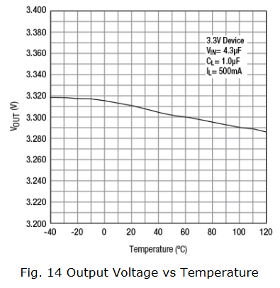
In addition to thermal shutdown, this chip has a negative temperature coefficient - as chip temperature rises, output voltage falls (graph from data sheet). The temperature axis is likely chip temperature rather than ambient temperature: output voltage vs. temperature graph from data sheet


I suspect there's a typo in that graph: \$V_{IN}=4.3V\$, rather than \$ V_{IN}=4.3uF\$

\$\endgroup\$

Your Answer

By clicking “Post Your Answer”, you agree to our terms of service and acknowledge you have read our privacy policy.

Not the answer you're looking for? Browse other questions tagged or ask your own question.