7
\$\begingroup\$

I'm designing a CAN bus interface for a PCB I'm working on. CAN and high speed/long distances are new to me, so I have a list of concerns about my design ideas, and I would appreciate someone with more experience than myself offering their thoughts, and hopefully criticisms.

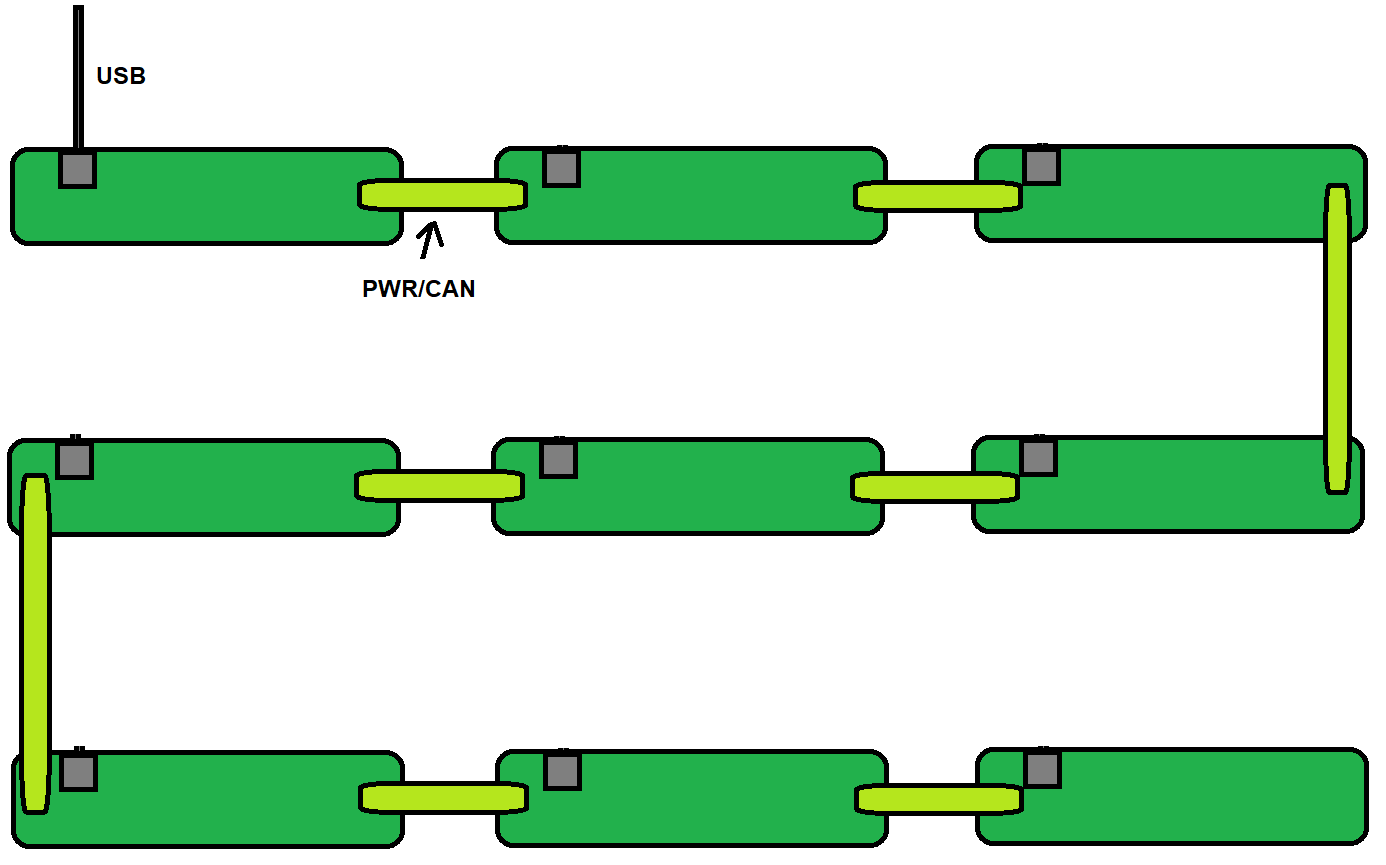
My design is a between 4-10 node network of 30cm long PCBs with CAN entering a connector on one side of the board, and entering the other. A connecting PCB will then bridge the CAN (and some power) to the next board. The first board in the network will always be connected to a PC via USB.

![enter image description here

The features I wish to reach with my design:

  • 1Mbps CAN
  • Automatic termination
  • Nothing blows up

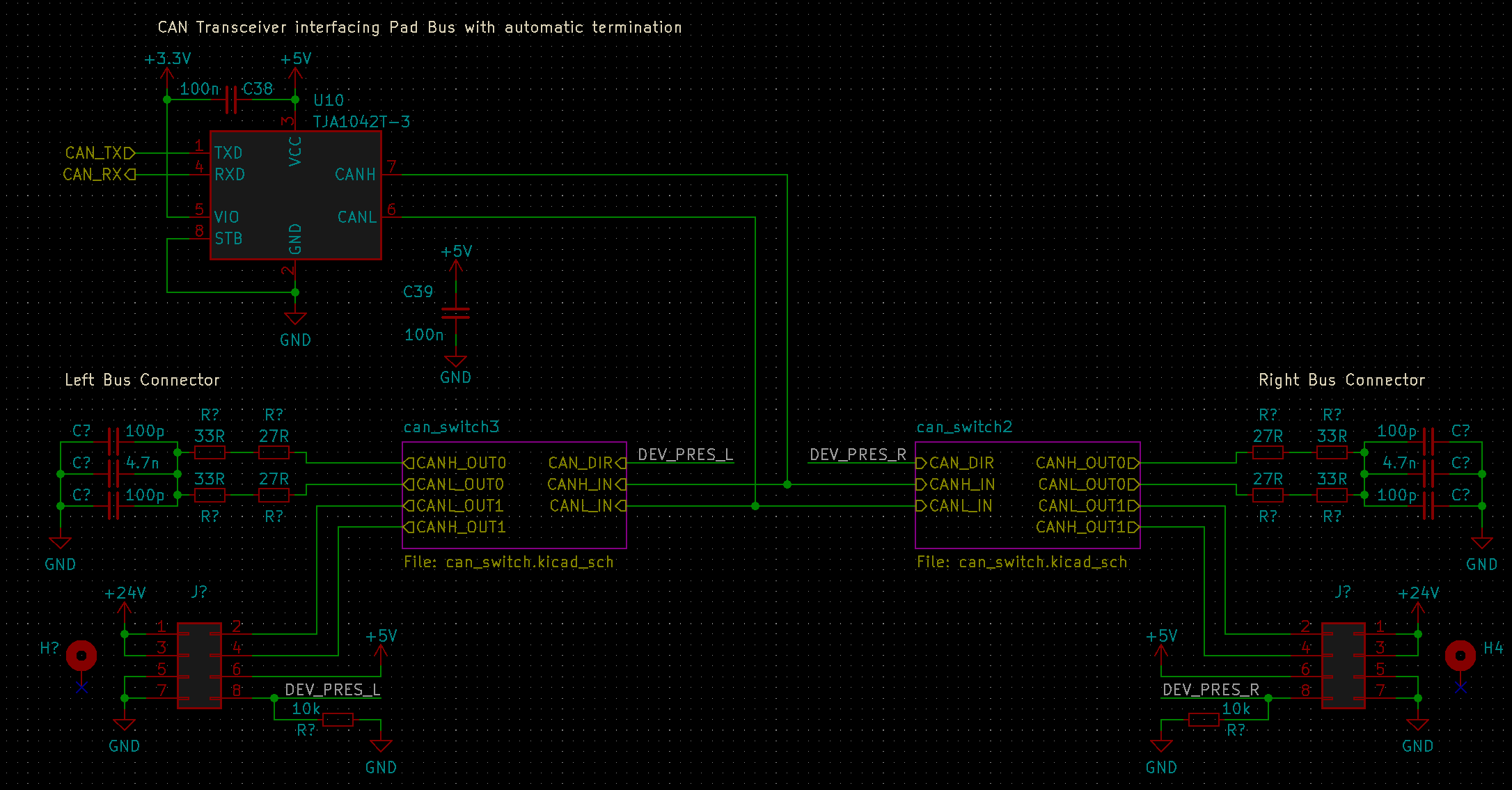
For that, here is my schematic -

enter image description here

I've got a transceiver for the node, which hooks up to two 'switch' units. Those units are supposed to choose whether the CAN signal goes to termination, or to another node PCB, on both the left hand and right hand side of the board. The connector boards act as a jumper for pins 6 and 8 on those bus connectors, and indicate that there is another node PCB.

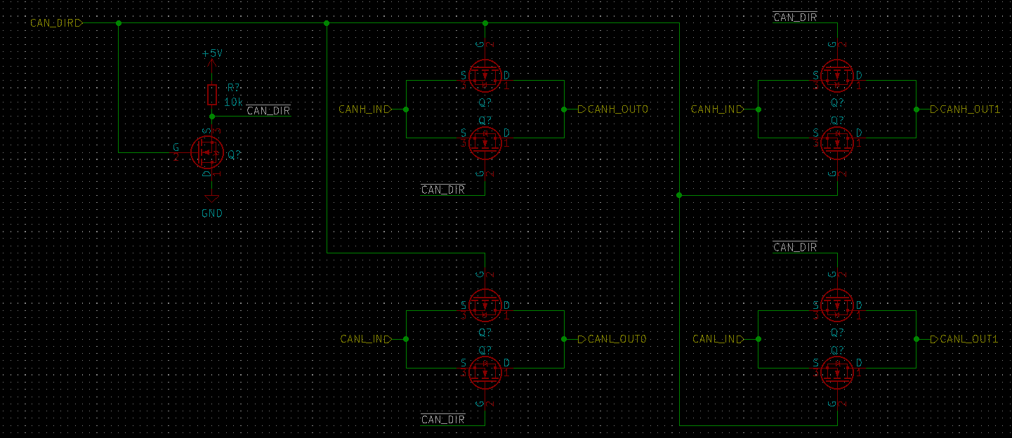
Here is the schematic for the switching unit:

enter image description here

I've chosen a CMOS pair, AO3400A and AO3401A with R_on of 45m. I've chosen to work with discrete components as no available analog mux to me appeared to have any reasonable R_on and I'm reasonably satisfied that the components account for voltage swing. Using the CAN_DIR and the NMOS-inverted CAN_DIR signals, I can choose to route CAN to channel 0 or channel 1. So that's what allows automation for whether we're connecting to a new node, or terminating.

This brings me to my requests for input -

  • I have no means/experience with high-speed interfaces to be able to tell whether or not my switching unit will allow me to accomplish 1Mbps. Have I introduced any unintended effects here, or are my CMOS capacitances/resistances reasonable? Have I created a topology here that makes sense?
  • I'm not working with twisted-pair cables. All CAN traces across the node PCBs and connector PCBs are impedance controlled to 120R, well isolated with ground plane separation, and the switch units introduce less than 1R to the network. Would it be reasonable to assume my bus length of up to 3 meters (with 2cm node stubs) will be effective for the 1Mbps requirement?
  • I'm lacking on the input protection. I haven't used any clamping diodes, nor TVS. This is because my MOSFETs and transceiver are reasonably well-rated already for ESD, and hot-swapping/user error is not a concern of mine given that these connectors are bolted down during assembly. Have I worked under some reasonable assumptions or is this still an everything-explodes risk?
  • Have I done anything dumb, here? Or is there anything you would do, as an engineer, to relieve some concerns? Any concerns you may have would be much appreciated.
\$\endgroup\$
11
  • \$\begingroup\$ Why do you use 27R + 33R? Just to meet E12 series? 2x60 ohm resistors would be cheaper. \$\endgroup\$
    – Lundin
    Commented Jul 8, 2022 at 9:50
  • \$\begingroup\$ As for protection, my experience is that most CAN transceivers on the market (especially recent ones) are very rugged and don't need external TVS. A common mode filter on the CANH + CANL lines isn't a bad idea however. \$\endgroup\$
    – Lundin
    Commented Jul 8, 2022 at 9:55
  • 7
    \$\begingroup\$ Also I have no idea why people are close voting this. Design reviews of schematics was always perfectly on-topic here, far as I know. \$\endgroup\$
    – Lundin
    Commented Jul 8, 2022 at 9:58
  • 1
    \$\begingroup\$ Thanks @Lundin, I often come here to see other people's design processes, and find it very useful when design is reviewed. :) I've chosen 27R+33R because it's cheaper through JLC's basic parts range. And I'll do my best to throw in a common mode filter! \$\endgroup\$
    – Brittany
    Commented Jul 8, 2022 at 10:24
  • 1
    \$\begingroup\$ Thank you for your responses. CAN is my choice as UART over RS-485 proved to have less error handling than my application required. I've made the decision not to have automated termination. Instead, I'll just have the left and right connector wired directly, and create a small terminating PCB to add to the start and end. Simple answers are always the best. :) \$\endgroup\$
    – Brittany
    Commented Jul 9, 2022 at 16:32

2 Answers 2

2
\$\begingroup\$

The switching network seems fairly complicated. I do not see why you need to terminate both the left and the right side of the bus per PCB. ALL you really need to do is pass the can signal straight through the PCB from connector to connector and add a single switching element to terminate the buss once per PCB.

You may be concerned about stub length... Since your PCBs will be ~30cm if termination is done somewhere close to the center you will have a stub of 15cm on the end of the BUS and that should not be a problem...

The switching elements you are using appear to be regular N and P channel mosfets. As your schematic shows these have internal bypass diodes as a consequence of their design. Since you have used these in parallel... They will always conduct.

\$\endgroup\$
0
\$\begingroup\$

Not an answer, but a formatted comment.

You'll also have to deal with addressing. If you are using a CAN, bus contention is resolved based on node address, where the lower the address, the higher the priority. So, you have to solve addressing you might as well also just do the auto termination.

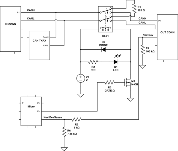
Instead of the FET switch, I would seriously consider a small signal DPDT relay near the "outgoing" connector side of the device. The COM terminals would be connected to the board's CAN traces, the NC terminals would have the 120Ohm terminating resistor, and the NO terminals would connect to the outgoing connector. The COIL terminals would have an LED indicator to show when energized.

The idea is that: when a new device is connected to the end of the chain, it pulls up(or down) the device presence pin on the IN connector, waits until the bus is available, then and starts broadcasting on an artificially low address, like 0x000 or something to request an address -- or you could even have it suggest an address if your module has a pre-programmed preference, the host responds on a new, artificially low address like 0x001 with the address it should use. The module configures itself with the assigned address.

When an upstream device detects a voltage change on the OUT connector's device presence line, waits until there is no communication on the BUS, asserts the dominant bit to halt communication, then it energizes the COIL allowing CAN to pass through. Once the relay is activated, it releases the CAN dominant state allowing the next module to request an address.

Here's what I'm thinking.

schematic

simulate this circuit – Schematic created using CircuitLab

\$\endgroup\$
2
  • 1
    \$\begingroup\$ CAN does not have "addresses", and there is no need to "obtain" one. Priority comes from the message being sent, and it is perfectly legal for two different devices (or boards) to produce the same message. Of course, may be that the OP has to do some sort of "addressing", but the term is wrong. \$\endgroup\$ Commented Jun 21, 2023 at 7:08
  • \$\begingroup\$ Regarding node ID assignment, I wouldn't recommend reinventing the wheel (20 years ago we had to find out the hard way). If it's CANopen, I would implement LSS. And if its some other application protocol, I'd still get my inspiration from CiA 305. It's tried and tested. \$\endgroup\$
    – Velvet
    Commented Jun 21, 2023 at 7:32

Your Answer

By clicking “Post Your Answer”, you agree to our terms of service and acknowledge you have read our privacy policy.

Not the answer you're looking for? Browse other questions tagged or ask your own question.