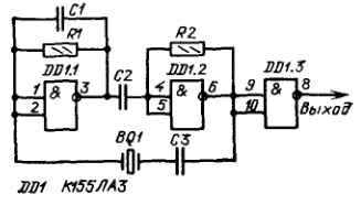
I have assembled a square wave generator following this schematic from an old book.
R1 and R2 are both 1 kohm, C1 is 68 pF, and C2 is 2.2 nF. The author of the book claims that this combination is suitable for working frequencies of 2 to 3 MHz. Capacitor C3 is to be selected during adjustments.
Instead of the К155ЛА3, I used a КР1533ЛА3, a later and improved version, differing in faster switching time and lower power consumption. Online shops and references give SN7400 and Texas Instruments SN74ALS00AN as analogues for those ICs. As for the structure, both of them contain four TTL two input NAND elements.
The assembled generator works, and the frequency is more or less stable 2 MHz, in accordance with the crystal resonator BQ1.
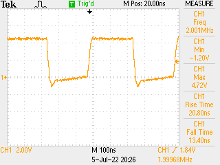
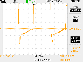
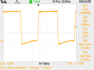
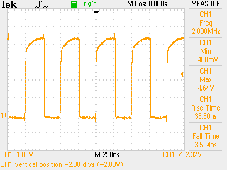
What I don't like at all is the output voltage going negative, as low as -1.2 V. Below are two plots from an oscilloscope, the second one showing the lower part of the signal zoomed in.
I tried fiddling with resistor and capacitor values, like decreasing R1, R2 to 470 ohm or increasing them to 1.2 kohm, setting C1 to 100 pF and C2 to 10 nF (that was another combination given in the book, stated to suit 2 MHz exactly), or selecting C3 between tens of pF and 68 nF. All of that only slightly affected the rise and fall time, but the low and high levels remained nearly constant, about -1 V and 4.7 V respectively.
Can I get the lower output level to correspond to TTL levels, say, something between 0 and 0.4 V? If yes, what should be changed about the circuit?
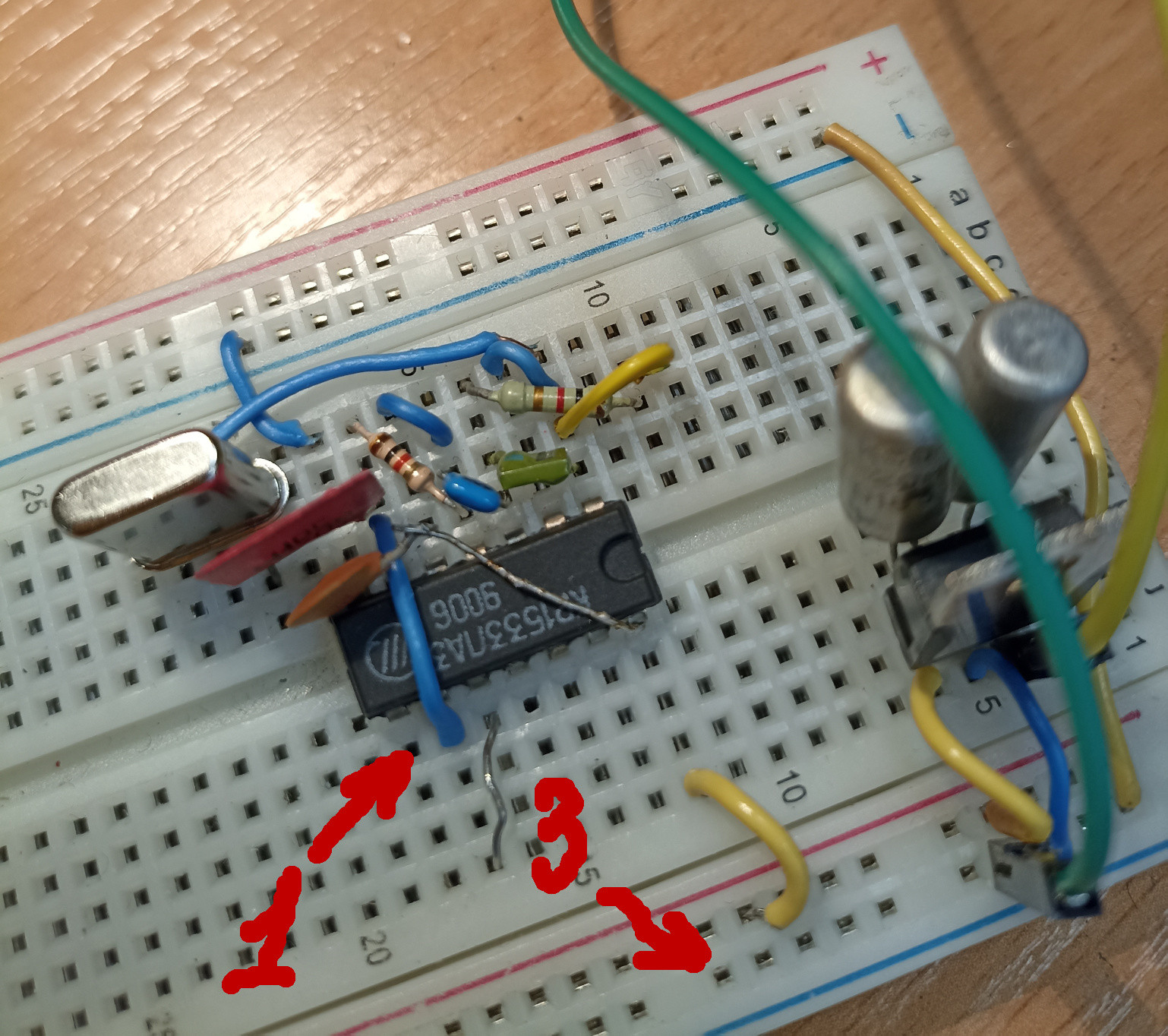
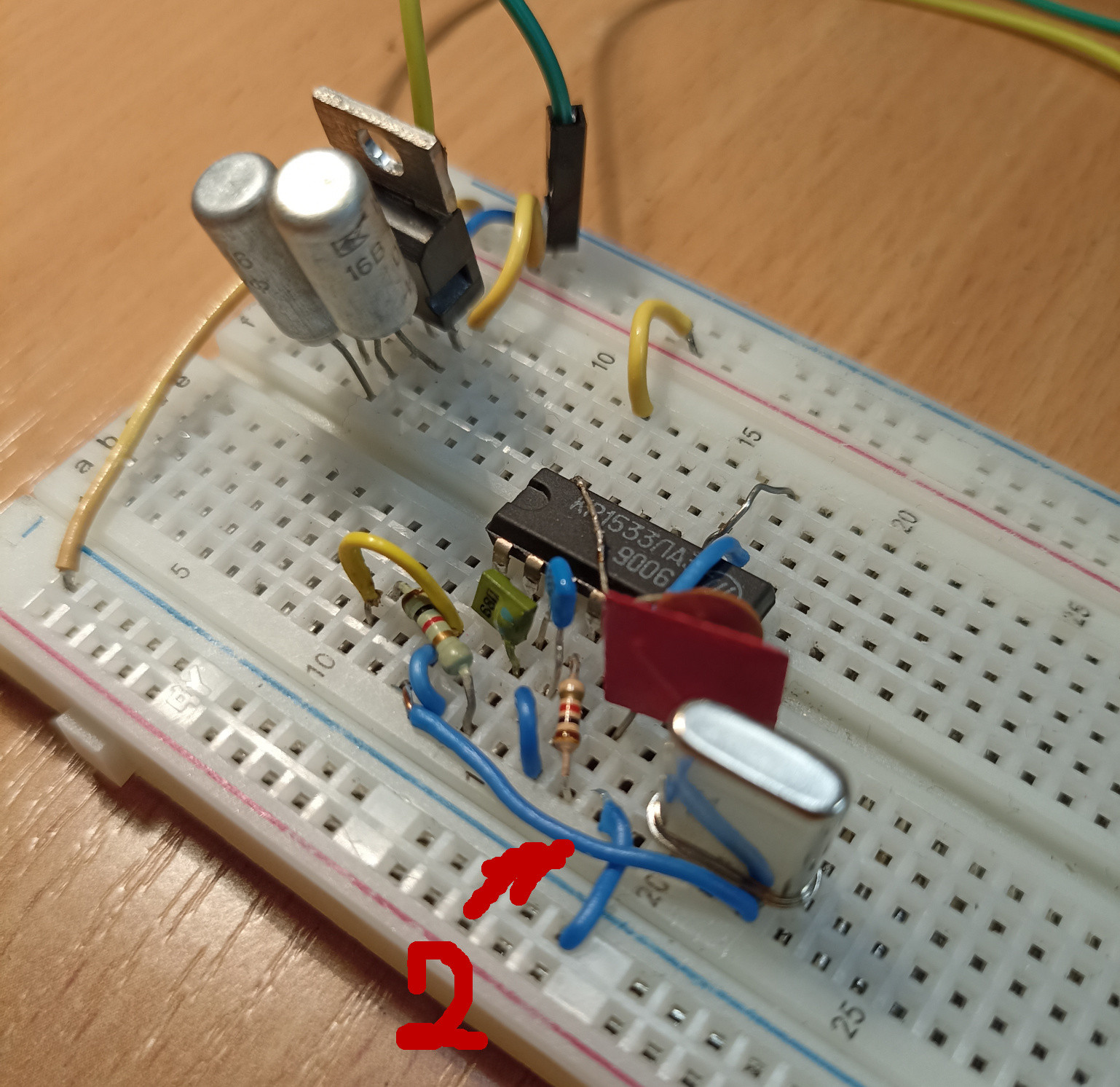
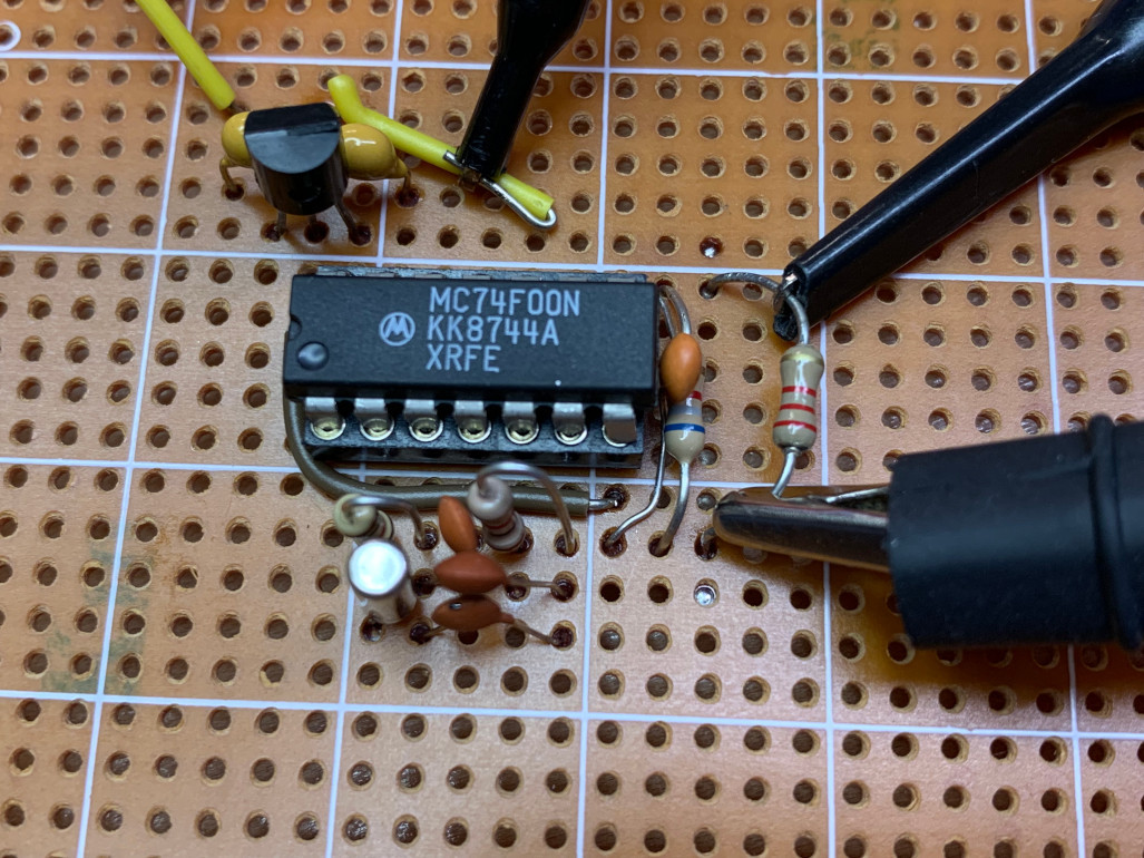
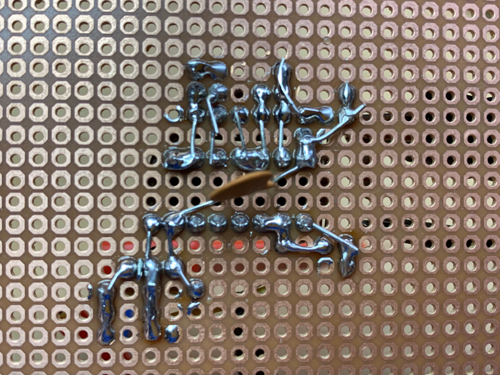
UPD: I have soldered a 0.1 uF ceramic capacitor right to the IC's power pins. Below are two photos of my circuit from two points of view. Sorry if the setup is hard to understand, it is actually pretty tight.
The circuit is powered by a 7805C regulator (in the corner of the breadboard,) with two 20 uF capacitors connected between its input / output and its ground pin (middle one.) The input power (yellow and green wires) is regulated 9 V from a lab source. I also tried setting the source to 5 V and connecting it directly to the IC, and that didn't change the circuit's behavior.
I connected the oscilloscope's input probe to the point labeled 1, and the ground probe to the point 2, next to the short blue wire going to the ground bus. Before that, I used to connect the ground probe to the bus, at point 3 for example. The probes are short hard pins held by crocodile clamps, did not photo them because they cover most of the circuit when in place.
The output is now about -0.5 V at its worst, which is not perfect but much better than before. I also tried connecting a 3.3 kohm resistor (the first one available at hand) from the output (pin 8) to the ground bus (the row marked by 3) and connecting the probes across that resistor. The numbers I got were nearly the same, so the load must not affect the circuit much, I suppose.
UPD2: The overshoot stays nearly the same (-480 to -560 mV), no matter if I change the capacitor on the power pins from 0.1 to 0.47 uF or disconnect it altogether. So the positive effect was mainly from repositioning the probes.
UPD3: I remembered about having a probe like that available and tried it.
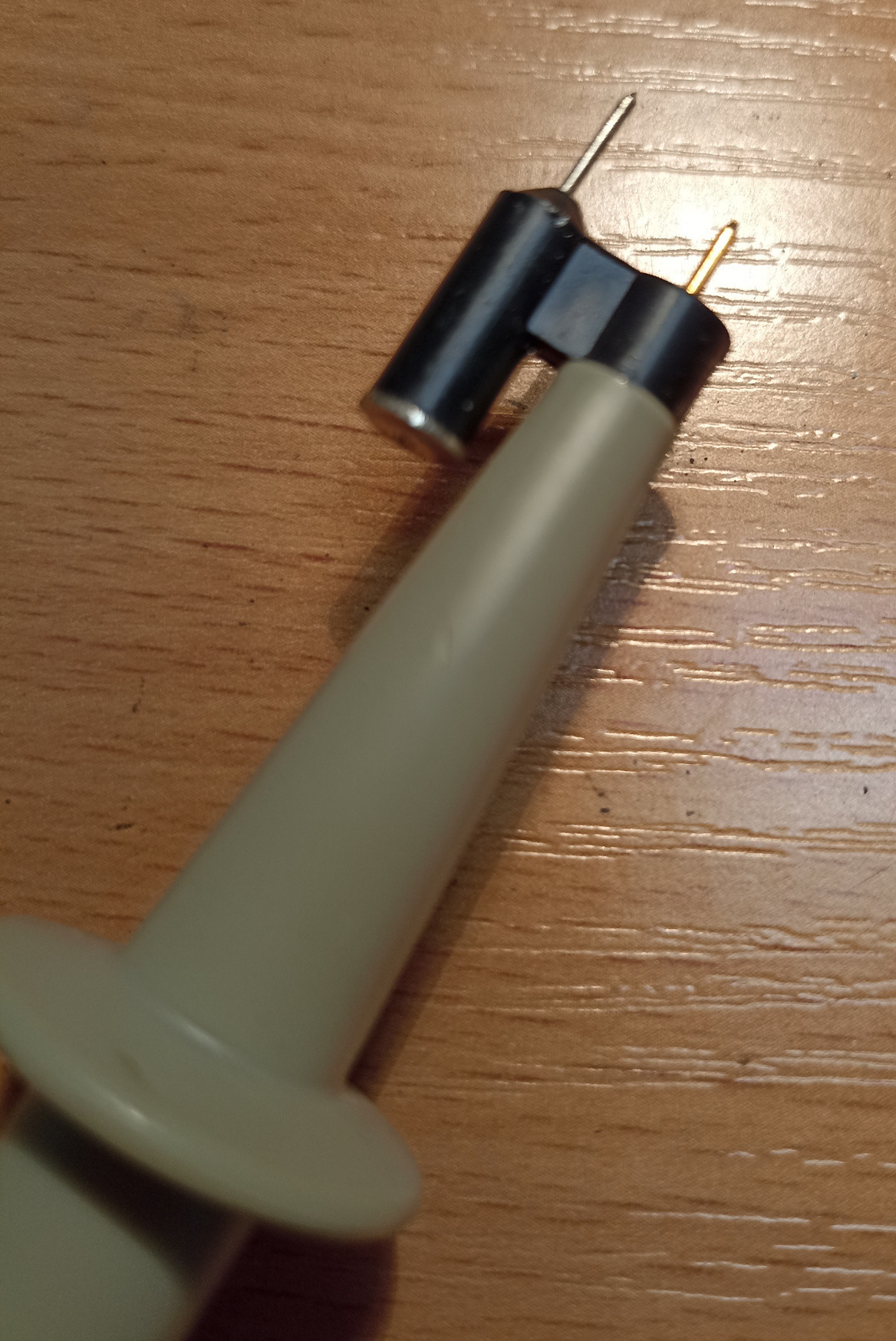 It has obviously the shortest connectors there can be. Also, it acts as a 10X voltage divider. After the calibration I got the following signal shape for a 0.47 uF capacitor at the power pins.
I tried increasing the capacitor to 1.5 uF, but got nearly the same result. It seems also that the signal's shape changed depending on how exactly I placed the probe, and the least overshoot I have seen was about -120 mV.
UPD4: Before I experimented without that RC couple between DD1.2 and DD1.3. Now I have added it, and the circuit behaved a bit better. I also tried adding a 220 ohms or 470 ohms resistor parallel to C2, and a similar one between IC's pin 1 and the quartz, as suggested by other similar schematics. Anyway, the best value I have seen was some -40 mV.
What I am thinking about is couldn't I influence the operating point of one or more logic elements, so that the signal "shifts" up?
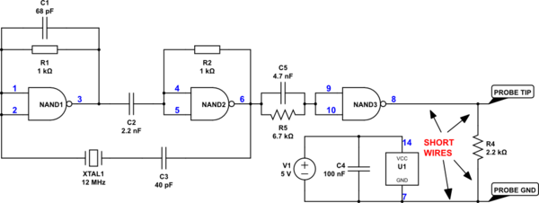
The final update: The idea to separate DD1.3 from the first two elements worked well, thanks once more. I also added some negative feedback to DD1.3, since there was none. So the circuit is looking like this now. C5 is situated near the voltage regulator, and C6 at the IC's power pins.
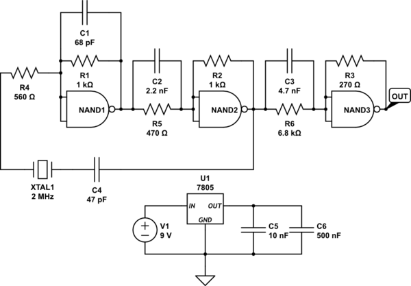
simulate this circuit – Schematic created using CircuitLab
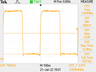
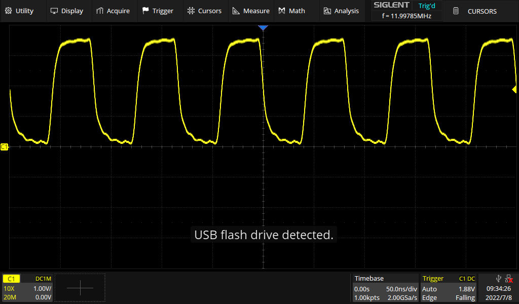
And this is the output signal. The minimum value (200 mV) was measured by those two downward "teeth", and the value at the horizontal cursor is about 320 mV.
Of course, the "high" level also got decreased because of the feedback, but I hope 3.2 V is pretty enough for TTL. Maybe after I reassemble the circuit using soldering it will need some more tuning, but now I know at least what to change.

