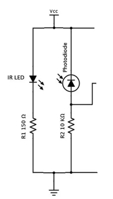
In practice, these devices get damaged very soon. (Some people that use this circuit report this problem).
If by "get damaged" you mean "they age" rather than "they get mechanically damaged", then you're just pushing the LED too hard. It may also be a crappy led, since 25mA through a 5mm LED is not a big deal normally.
Drive the LED at average current below 50% of the recommended operating current and it will last "very long" - definitely much longer than the current design. You can always make the detector more sensitive. 3.5cm is nothing for a LED-photodiode combo used as an optical interrupter. You can be driving that LED with a 100uA 1-10kHz square-wave and detect the output from 3.5cm away no problem using any 4x4mm photodiode, a transconductance amplifier and synchronous detector. With such low drive, the LED will last longer than your and my lifetime added together. I.e., for practical purposes, the LED lifetime is infinite at such low drive currents. Even for crappy LEDs.
The photodiode+resistor detector is a very crude circuit and not very sensitive. This relative insensitivity of the detector is the big part of your problem. Making the circuit use synchronous detection will not only let you detect smaller signal, but also improve the noise rejection.
The whole thing can be made using a 555, a quad op-amp, and a DPDT analog switch. The parts cost a couple of dollars in very small quantities.
A tested design is shown below. I'm using a RED led of the same type for the transmitter and receiver, but it can also be an IR LED of course. No need for a specific photodiode, although a photodiode would improve the sensitivity.
The circuit is not particularly sensitive to low frequency ambient light. It rejects DC light, so it works in full sunlight. It can tolerate partial illumination with a bright PWM pencil flashlight, and works under all reasonable indoor lighting conditions. With visible light you can at least visually confirm that the beam source works.

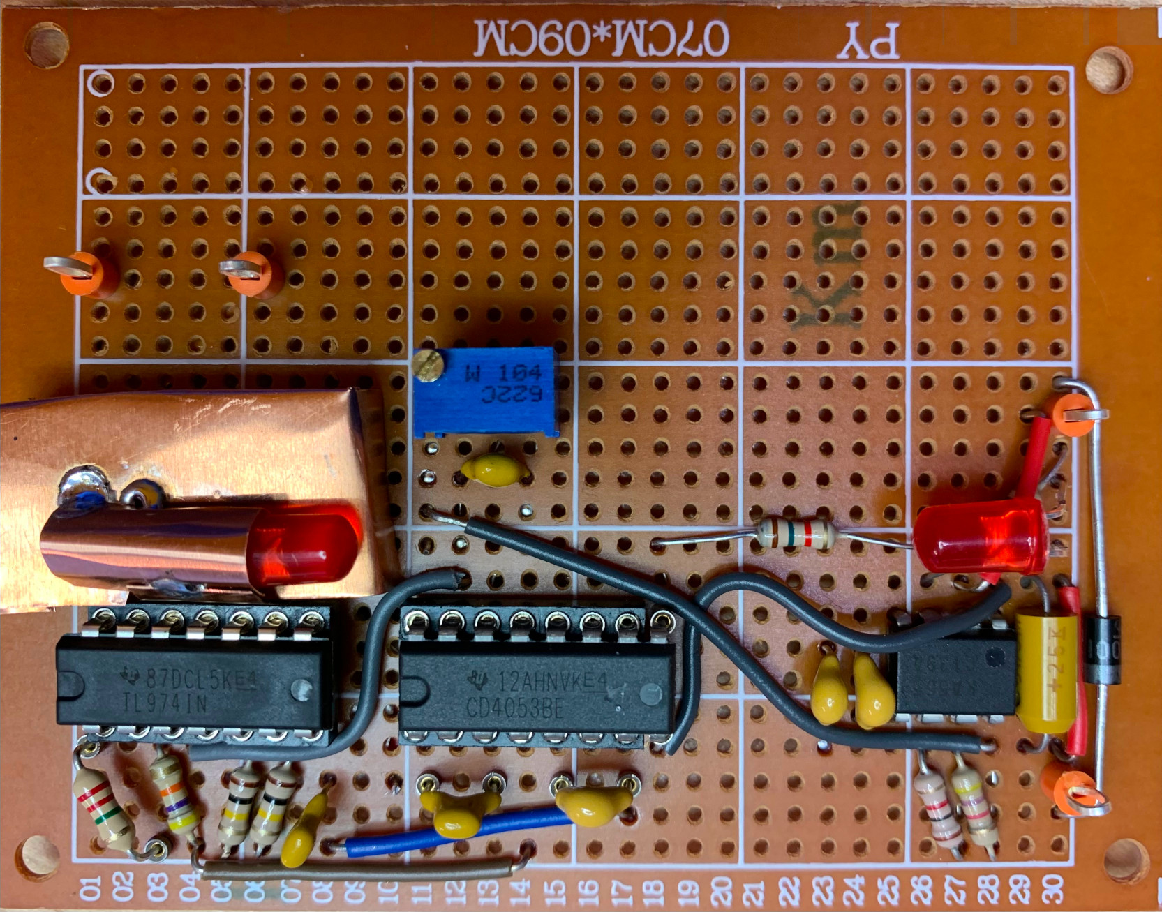
The chip lineup is all-TI:
- U1: CD4053BE
- U2: TLC555CP
- U3: TL974IN
U2 is a simple oscillator with rail-to-rail output. The rail-to-rail output is important, as it controls the CMOS switch. R4 reduces the slew rate of the control signal reaching the switch, and minimizes electrical feedthrough from the transmitter to the receiver.
U3A is a transimpedance amplifier. It biases the receiver photodiode at VCC/2. U3B is a 100x AC amplifier. U1A/B are the demodulator switch and filter. C8 is the flying capacitor. C9 is the integrating capacitor. C9 is fairly large, and can be made smaller - say 1uF - to speed up the response. U3D is a buffer for the reference voltage needed by the demodulator to output centered at VCC/2 and not at VCC, outside of the op-amp's common mode range. U3C is the final DC amplifier. It could be followed by a CMOS schmitt buffer, like CD40106. The output is rail-to-rail and compatible with either TTL or CMOS inputs. For TTL, the fanout is 1.
A legacy 5mm LED is not a particularly sensitive detector, due to its small area, so a lot of gain is necessary. For a larger photodiode, the gain of the 2nd preamp stage can be lowered, as well as the transimpedance of the 1st stage.
VR1 should be adjusted for 0.5V output voltage with the transmitter or receiver diode covered. The output is active high.
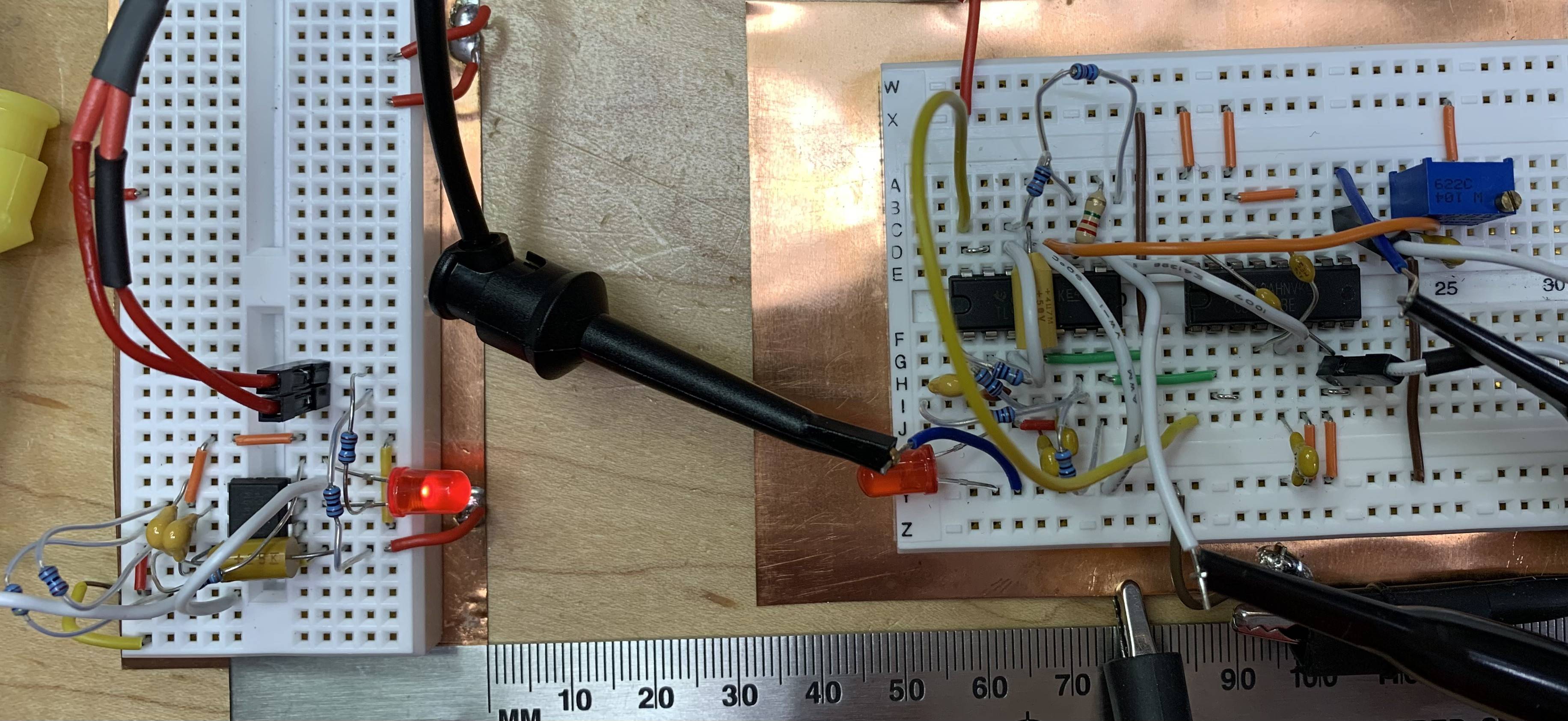
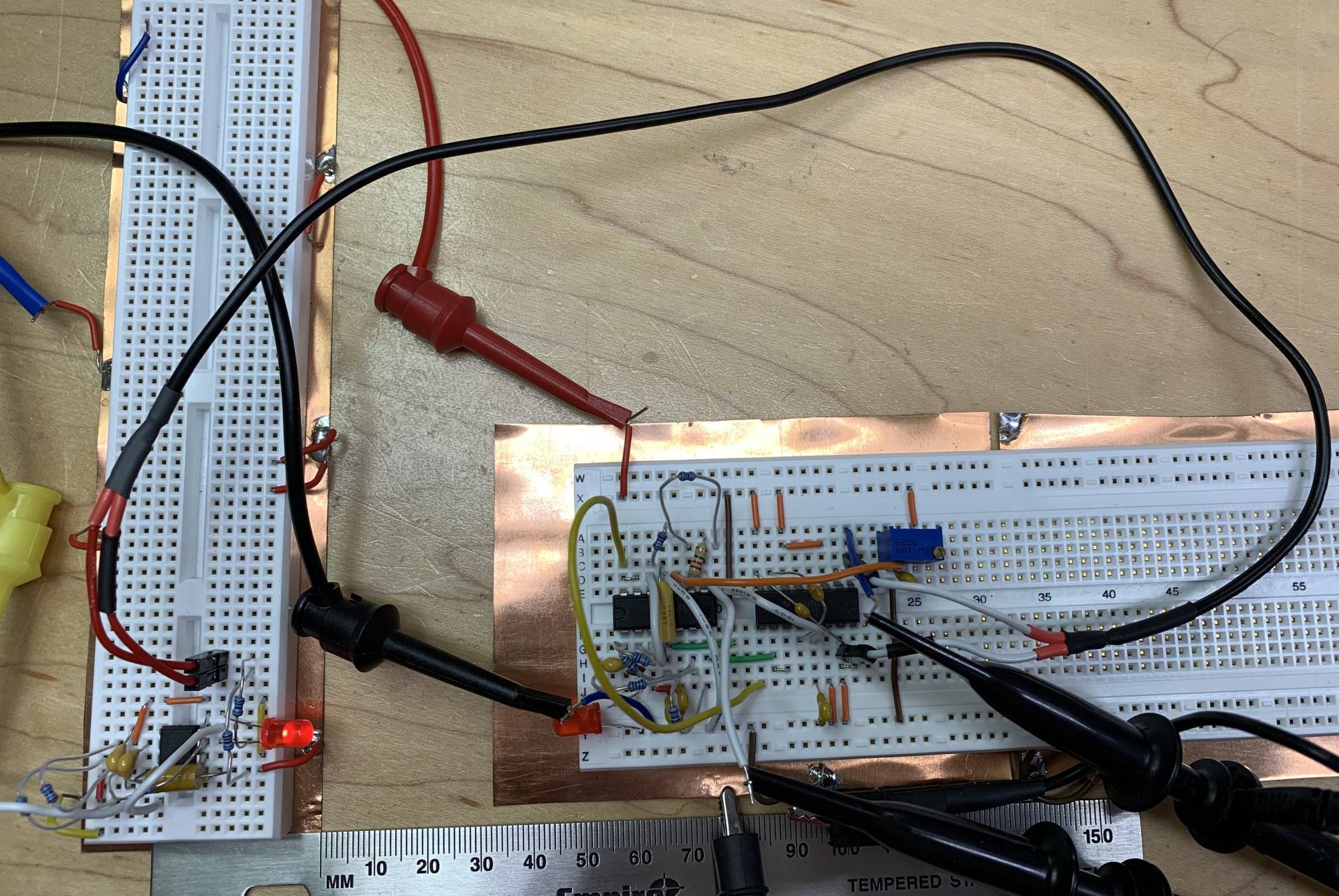
The PCB layout should have a separate ground plane for the transmitter and the receiver, connected at a single point. This circuit is hard to get to work without shielding on a breadboard - the copper shield on the bottom of the breadboard is a must. The overall voltage gain of the 2nd and 3rd stage combined is about 5,000. The transimpedance is about \$5{\,\rm V}/{\rm nA} = 1{\,\rm V}/{\rm\mu A} \cdot 5000{\,\rm V}/{\rm V}\$.
There are several high-impedance, sensitive current summing nodes. The clock connection between the transmitter and the receiver is a 1ft shielded cable. R4 is split into two halves, one in series with the shield, the other in series with the center conductor, on the transmitter side. The shielded cable connects directly between GND and control inputs of the switch U1.
The supply range is 4.5V to 12V. The voltage should be regulated, as large changes require adjustments to VR1.


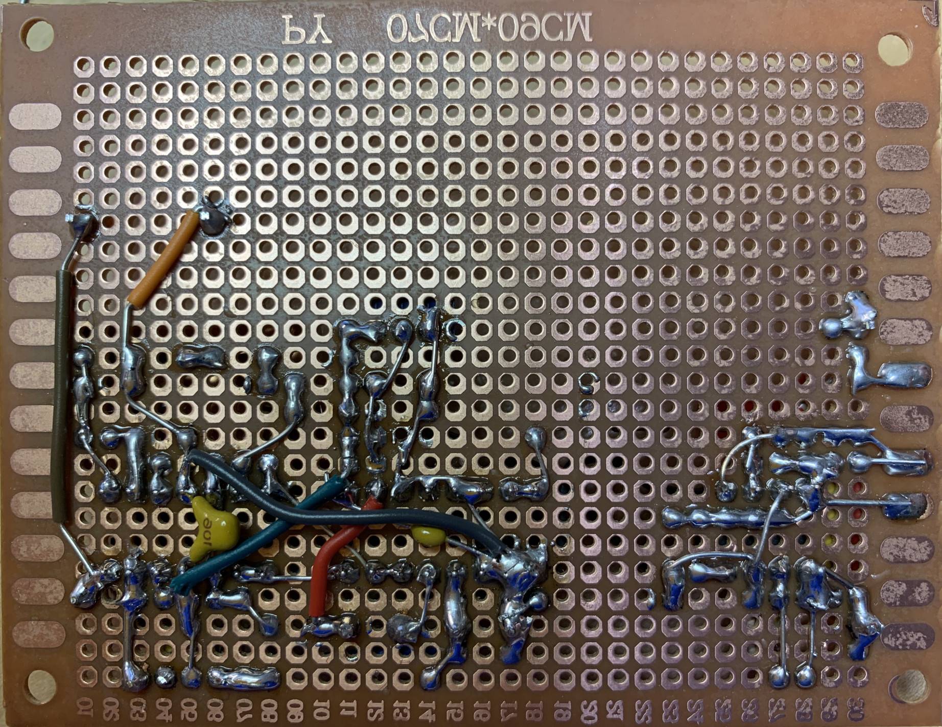
I've also assembled it more permanently on a single breadboard. Note the shielding needed to make the receiver insensitive to interference from other nearby circuits/devices that may be in the enclosure:
