1
\$\begingroup\$

Can you explain the basic reason why boost converters seem to be more popular than voltage doubler circuits for load bearing output?

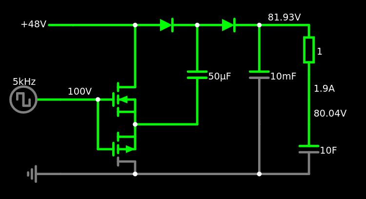
I have built these two circuits in the simulator and they both basically achieve the same result of charging an 80 V battery from a 48 V supply.

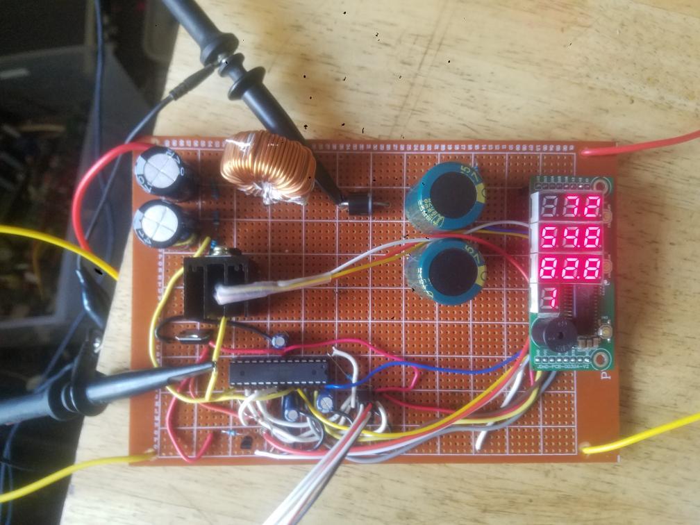
I have built the boost converter on a circuit board and wasted many hours blowing up MOSFETs and making the circuit work on a real-world circuit board with reasonable success.

I have also built a voltage doubler circuit that achieves producing the desired voltage output but only when not under any real load. Yet in the simulator it works as well as the boost converter.

What are practicality / lifespan / cost reasons why boost converters are used for high current voltage doubling? Is there any point in me persevering with making my voltage doubler circuit work properly?

It is all a learning curve really but it would be nice to be able to actually charge my 80 V battery at the end of it.

So far I can charge the battery at 1 A with my home made boost converter as long as I remember to unplug the input power before the output power, it blows the MOSFET if I disconnect the output while its running, but I think that's a microcontroller issue not responding to the rise in voltage fast enough when the load is disconnected and the PWM duty becomes to high, that I should be able to overcome if I think about it.

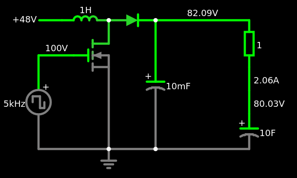
Boost Converter

Voltage Doubler

Home Made Boost Converter

\$\endgroup\$
10
  • \$\begingroup\$ A boost converter either needs feedback, or a load. Or, the output will rise until something fries. \$\endgroup\$
    – Mattman944
    Commented Jul 31, 2022 at 22:24
  • 6
    \$\begingroup\$ Applying 100 volts to the gate-source of a MOSFET is deserving of a down vote (based on not actually doing any research into what a MOSFET can handle). Sorry if this sounds harsh but, it's a fundamental reality you have to take on the chin as part of your learning curve. A 1 henry inductance for the boost converter is also miles away of what would be needed at a 5 kHz switching frequency. And, there's no way that the inductor in your picture is 1 henry so, there are glaring errors in your question that would take pages and pages of text to explain. Start a lot simpler. \$\endgroup\$
    – Andy aka
    Commented Jul 31, 2022 at 22:24
  • 1
    \$\begingroup\$ thanks for the feadback, your correct the circuit simulation is not the same as my PCB, i am playing around with the simulator trying to understand things before blowing them up on the PCB. i honestly dident realize it mattered that much, I do not have 100v at the MOSFET gate but in the simulator it makes no difference so i failed to notice, i was just trying to explain what i was on about with pictures rather than words. if it was you that left the negative feedback than next time please have the decency to explain why before rather than after, i have nothing i can learn from no explanation. \$\endgroup\$
    – Jay Dee
    Commented Jul 31, 2022 at 22:41
  • 2
    \$\begingroup\$ @JayDee No, you're reading the MOSFET regions of operation improperly, or incompletely. The voltage across the source-drain drops as the MOSFET conducts more and that's what causes the gate-source voltage to become higher than the drain-source voltage. It's not something you do to the MOSFET, it's a result of applying sufficiently high gate-source voltage. There's a bunch of moving parts going on and depending on the circuit things will "settle" at some mode of operation. \$\endgroup\$
    – DKNguyen
    Commented Jul 31, 2022 at 22:51
  • 5
    \$\begingroup\$ @JayDee The voltage rating of a MOSFET refers to the drain-source voltage. The gate-source voltage is usually limited to much lower voltages; I've never seen ones rated above 20 V and most non-WBG MOSFETs are recommended to be driven with 10 V on the gate. Further, your average MOSFET can handle limited drain-source breakdown, and some are even rated for it (this is given in datasheets as "avalanche energy", a rating of how much energy the FET can absorb in a single D-S breakdown event), but gate-source breakdown will destroy the FET instantaneously. \$\endgroup\$
    – Hearth
    Commented Aug 1, 2022 at 0:31

3 Answers 3

3
\$\begingroup\$

Both topologies are used. In very low power applications you can find charge pump circuits like the capacitive voltage doubler, but the more power must be converted, the more likely you see inductors in the solution.
There are big differences to deal with:

An inductor based converter applies a voltage across the inductor and let the current rise linear. This voltage must be turned off before the inductor saturates or the current rises excessive and destroyes the switch. You seem to have experience with this effect. The amount of energy stored in the inductor is controlled by the time the voltage is applied.

In a charge pump converter you have a very large instant current when the switch connects the pump capacitor. In low power converters with capacitors below some uF the switch cost is affordable, but even in your example circuit this current is above 100 A using a good capacitor. However the amount of enery stored in the capacitor can not easily be controlled, there is no linear dependency between charge time and energy.

The regulator options are also very different:
When the inductor current is turned off, the magnetic field collapses and this produces a voltage across the inductor. If there is no load, this voltage is very high, in practice typically 20 to 100 times the supply voltage used. You seem to have some experience with this effect too, you mentioned a MOSFET breakdown at the moment of load disconnect. So a boost converter must know the output voltage and calculate the next needed active time of the switch. That is close to zero if the target voltage is reached.

Since the charge pump doesn't know the energy transferred per cycle, it can only control the frequency of the cycles and monitor the result. The maximum output voltage is twice the input voltage, so there is no dangerous high voltage using a free running frequency. This is a typical use case, where split supplies for OpAmps or line drivers must be created from a single supply and only a few mA current are required.

My last point is the choice between useful components for the two topologies:
In the mW range an inductor is bigger and more expensive than the equivalent capacitor needed, and if no fast regulation is required, a charge pump is used with the benefit of better EMI values. But if you need capacitors above 100 uF, the charge pump solution becomes expensive. All electrolytic capacitors have a short lifetime compared to inductors and ceramics are not available in this range. Inductors however exist in almost any power range.

\$\endgroup\$
2
\$\begingroup\$

A boost converter regulates its output, while a doubler only (tries to) doubles. If the doubler is loaded, then of course the output voltage will fall (or if the input voltage falls), but any time the loading decreases the output voltage, then the efficiency drops. This is because while the input current is always twice the output current, the output voltage is not necessarily twice the input voltage.

Conversely, a boost converter regulates the output voltage the desired value, irrespective (within reason) of the input voltage or output loading. This type of converter may be over 90 % efficient.

\$\endgroup\$
8
  • \$\begingroup\$ A boost converter regulates its output? what do you mean? i have a microcontroller controlling the PWM duty cycle of my boost converter that is doing the regulating of the output by only charging the inductor when needed. I have a microcontroller doing exactly the same thing charging a capacitor as charging the inductor? surly if i only half charge the capacitor by cutting the power half way through i will only get half the voltage doubling (less diode losses). i just don't understand the difference \$\endgroup\$
    – Jay Dee
    Commented Jul 31, 2022 at 22:14
  • 5
    \$\begingroup\$ The boost circuit that the OP posted is open loop, no regulation. These are not as useful as a converter with feedback, but they do have their uses. \$\endgroup\$
    – Mattman944
    Commented Jul 31, 2022 at 22:20
  • 1
    \$\begingroup\$ @JayDee Have you actually tried to only "half charge" the capacitor"? Good luck with that. It sounds like you don't know why an inductor is generally there in switching converters. It might be obvious in a boost converter, but it is still there in a buck converter and the boosting is obfuscating the reason an inductor is generally there in all switching converters. First, examine the basic operation of buck converter and what the inductor does. Then allow me to propose you do away with the needless inductor and simply half charge a capacitor to regulate the voltage down. What's the problem? \$\endgroup\$
    – DKNguyen
    Commented Jul 31, 2022 at 22:30
  • 3
    \$\begingroup\$ @JayDee. You're wrong. 1) Your MCU doesn't 'know' when inductor charging is needed (or completed !). 2) While you can attempt to 'half charge' the capacitor a) this is difficult with a circuit that may have been designed to be reasonably efficient, and b) this alone is extremely inefficient -- it's not really a doubler in a conventional sense. \$\endgroup\$
    – jp314
    Commented Jul 31, 2022 at 22:46
  • 2
    \$\begingroup\$ @Hearth - Of course and I agree fully. But the OP has a primitive implementation and claims an MCU will control the output. The details of this are not shown. \$\endgroup\$
    – jp314
    Commented Aug 1, 2022 at 0:48
1
\$\begingroup\$

Voltage doublers are usually used for sine wave applications, Your voltage doubler will cause the capacitor to charge through the MOSFETs without any current limiting. If you observe these currents in your simulation, you will see currents that are far above the pulse peak current rating of the MOSFETs. Also there may be a finite amount of time where both MOSFETs are conducting. I'll do a simulation and come back later with more definitive results and perhaps an answer with a way to design a reliable voltage doubler that will work on a square wave. But it may wind up as more of a boost converter with inductance.

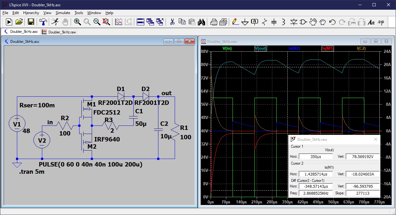
OK, I ran a simulation with a 5 kHz square wave and it does not look all that bad, except for the initial transition which causes a current spike of about 140A. After that the spikes are about 30A, and power dissipation in the MOSFETs is less than 5W, for an output of about 84 VDC into 100 ohms - about 72 watts. The MOSFETs have about 500 mOhm RdsON, and that accounts for the initial charging of C1 and C2.

Adding a 100 ohm gate resistor and 2 ohms in series with C1 tames the current surges to about 15 amps. The output is now about 80 VDC or 65 watts, with input of 77 watts and R3 dissipating 7 watts.

Voltage Doubler 5 kHz

\$\endgroup\$
5
  • \$\begingroup\$ thanks for the input, i would like to build this circuit, mostly for comparison to the boost converter i have built, rather than needing it to work. the 5kHz pulse is not critical, it is a microcontroller and can be any PWM duty that best fits. and the input is actually a 14 cell Lithium iron phosphate battery that can reach 57v so the input needs to be 60v tolerant. and the output is 24 cell liFePo4 so 86v. The microcontroller knows every individual cell voltage so it is capable of cutting the current if needed. the complete circuit is an 80v electric van + additional 55v portable power packs \$\endgroup\$
    – Jay Dee
    Commented Aug 1, 2022 at 9:06
  • \$\begingroup\$ i have a lot of 55v 3kwh lithium iron battery packs, the aim is to be able to charge my electric van off the portable packs i already own, i have it working at a few amps with my boost converter but that's not much power for a 200 amp EV, its far from real time power. im just experimenting for the learning curve really though \$\endgroup\$
    – Jay Dee
    Commented Aug 1, 2022 at 9:13
  • \$\begingroup\$ If you go with this approach, you would probably want to use a more conventional half-bridge with a pair of NMOS devices. You would also need to pick the capacitors to withstand the high peak currents, or minimizing them by some means. You might not need the output capacitor if the load will be a battery pack, but you will need to limit the current to a safe level. An output inductor might help, but it may be bulky. \$\endgroup\$
    – PStechPaul
    Commented Aug 1, 2022 at 20:35
  • \$\begingroup\$ would i be better off using 2 PWM signals to allowing for a delay between the 2 MOSFET switches possibly with an and gate to ensure both can not accidental be on at the same time? or would that cause other problems, \$\endgroup\$
    – Jay Dee
    Commented Aug 2, 2022 at 10:35
  • \$\begingroup\$ You can get half-bridge drivers that have internal cross-conduction protection. So a single PWM signal can be used if one input is non-inverting and the other is inverting. Otherwise you can generate complementary PWM waveforms with programmable dead time. As there is no inductor, you don't need to be concerned about handling inductor energy when both drivers are off. \$\endgroup\$
    – PStechPaul
    Commented Aug 2, 2022 at 20:21

Your Answer

By clicking “Post Your Answer”, you agree to our terms of service and acknowledge you have read our privacy policy.

Not the answer you're looking for? Browse other questions tagged or ask your own question.