1
\$\begingroup\$

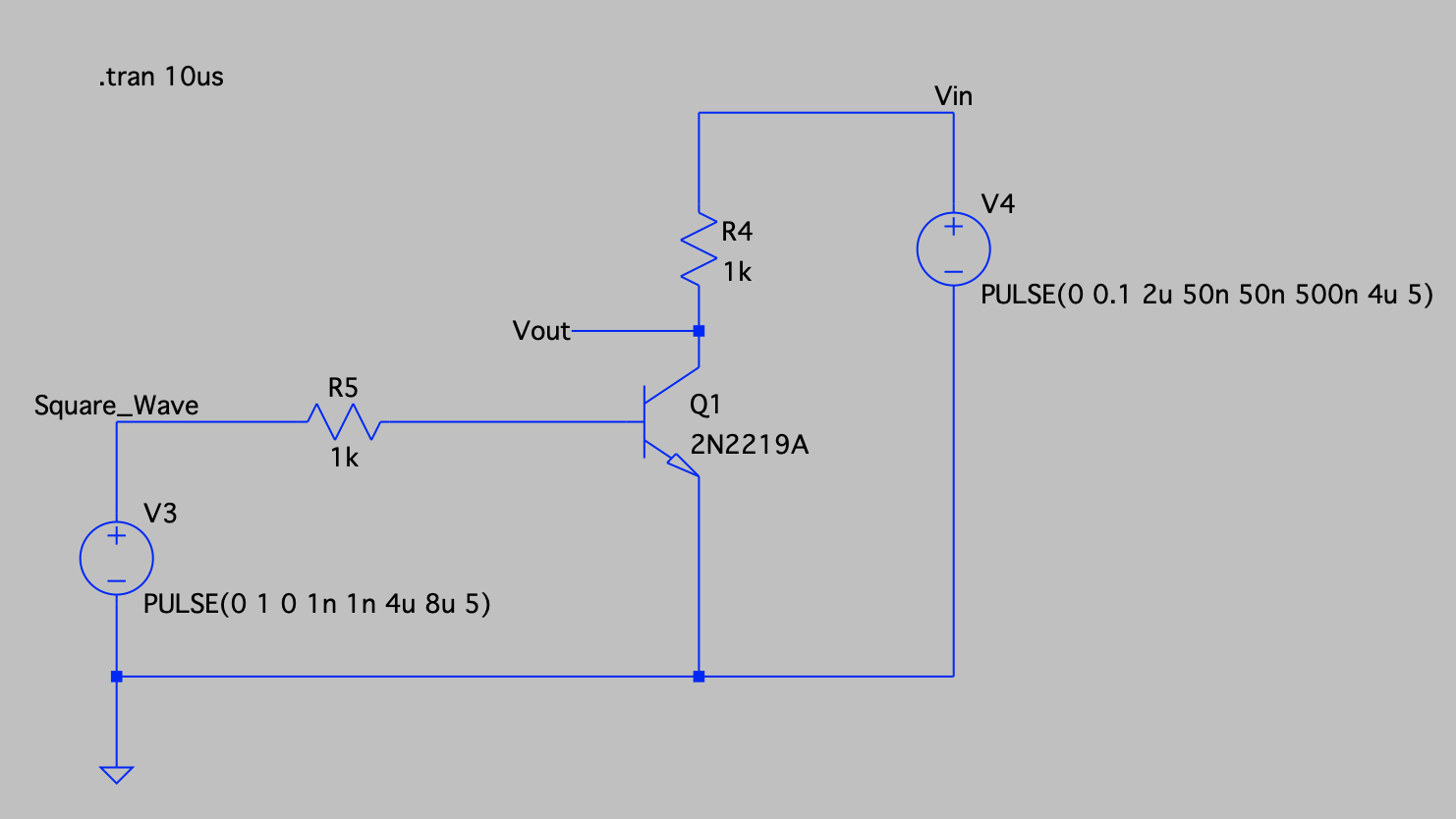
I've simulated a circuit in spice depicted below. The Vin voltage source (on the right) outputs a 100mV pulse every 2 microseconds, and the other voltage source (on the left) is a square wave that alternates between 0V and +1V. The idea is that when the square wave goes high, the transistor should turn on and cause Vout to equal zero, and when the square wave goes low, the transistor should turn off and cause Vout to equal Vin.

The circuit simulation in spice with a BJT

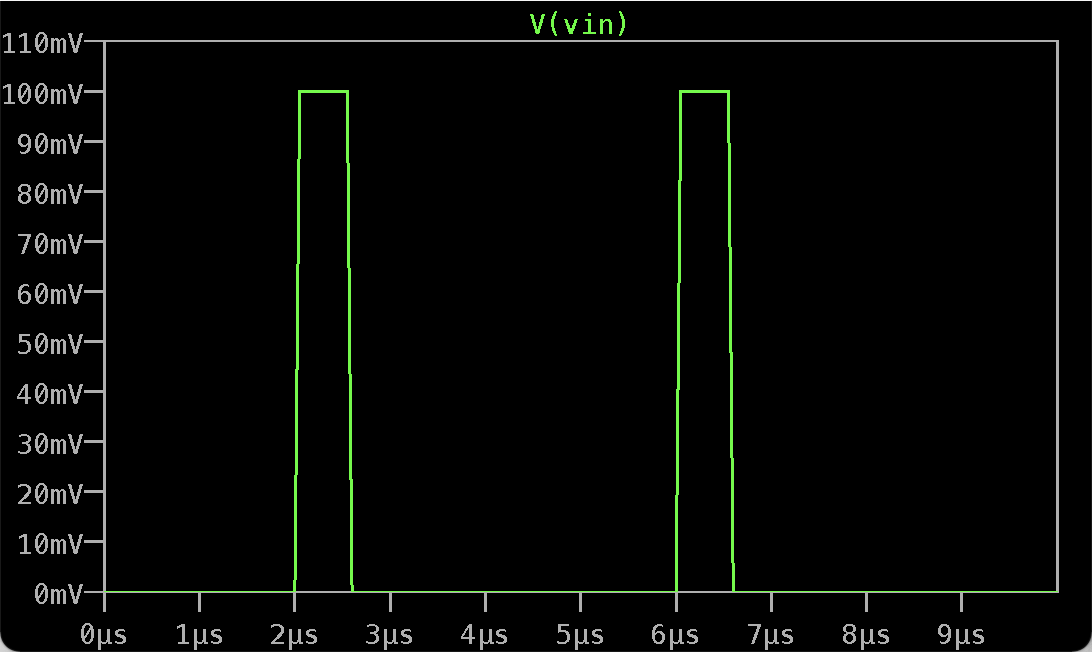
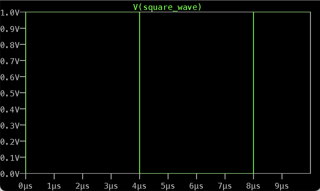
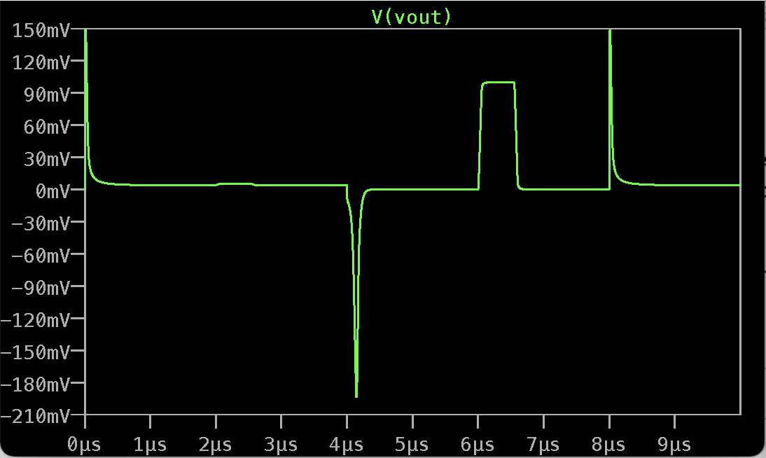
Here are 3 traces I recorded, depicting Vin, the square wave, and Vout:

Vin voltage trace Square wave voltage trace Vout voltage trace

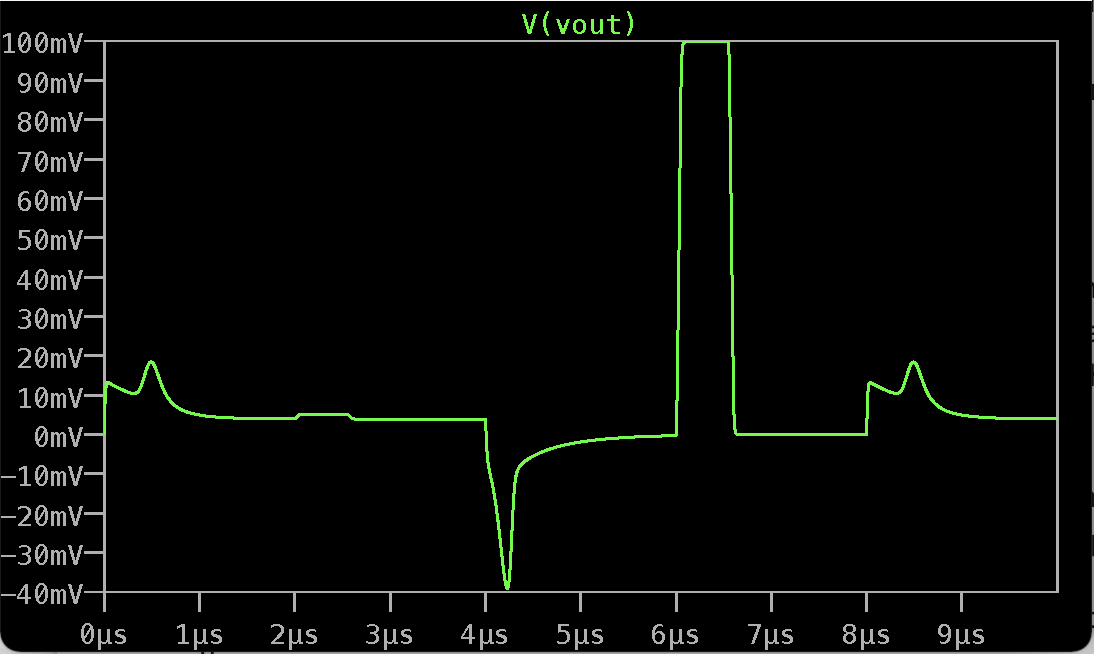
While the circuit is mostly behaving the way I expected, there is a large unwanted voltage spike at Vout that appears whenever the square wave has a rising edge or a falling edge (appearing at 0us, 4us, and 8us). My main question is, what phenomenon is causing these voltage spikes to appear at the output? Is there a name for this phenomenon? And more importantly, what can I do to get rid of it?

Would using a different type of bjt help? I have tried that but it didn't change much. I also tried using a mosfet instead of a bjt, but the voltage spikes were still appearing. Would a mosfet be more appropriate for this type of circuit?

I did notice that putting the square wave through a low-pass filter makes the voltage spikes smaller, but doesn't completely remove them. If I try it (by adding a 1nf cap at the BJT base), this is the result:

enter image description here

Does anybody know if there are other solutions that would work better?

\$\endgroup\$
5
  • \$\begingroup\$ Either decrease the parasitic capacitance in the transistor or slow down the edge. \$\endgroup\$
    – DKNguyen
    Commented Aug 1, 2022 at 1:05
  • \$\begingroup\$ IMHO, questions like this need to be presented in terms of real world application and intent, versus purely academic and theoretical concepts and curiosity. In this case the 1 nS pulse transitions are unrealistic outside of laboratory conditions, and all sorts of parasitic elements such as capacitance and inductance will have a major effect. \$\endgroup\$
    – PStechPaul
    Commented Aug 1, 2022 at 6:56
  • \$\begingroup\$ I actually am using this circuit in laboratory conditions. I'm using this delay generator module (thinksrs.com/downloads/pdfs/manuals/DG645m.pdf) which specifies a rise time of <2 ns or <1 ns, on page viii. Though I agree that this is a pretty unusual situation. \$\endgroup\$
    – Svedberg
    Commented Aug 2, 2022 at 7:15
  • \$\begingroup\$ If you could update your post with the suggested (1) Output loading (Capacitor + Resistor); (2) Increasing rise/fall time of Square waves; (3) Combined effect with “1+2”; they would show actual improvements using your initial models. All this would be greatly appreciated. \$\endgroup\$
    – EJE
    Commented Aug 2, 2022 at 16:29
  • \$\begingroup\$ While it is true that generator can create 1ns rise times, it comes with limitations (see page 115). Your internal impedance is 50 Ohms. It also has a current limit of 200mA. Implementing both of these will make your simulation much more realistic. However, modeling the load of this circuit at Vout (especially if it's 50 Ohms) is likely to be the biggest thing to make the simulation closer to reality. \$\endgroup\$ Commented Aug 3, 2022 at 0:42

1 Answer 1

6
\$\begingroup\$

You can't. There is generally some level of parasitic capacitance between the base and collector that will always allow some bleedthrough. This phenomenon is called "Miller Effect" and you can't get rid of it.

However, all is not lost. Your circuit probably isn't as bad as the simulation makes it look.

First, a 1 nanosecond rise or fall time on Square_Wave is far too fast. Unless you have specifically set up the circuit to cause that, very few real signals are going to be that fast. You should adjust that to look more like your real circuit implementation.

Second, you aren't modeling the "load" at Vout. Right now, there is no capacitance on it that has to be charged so it's really easy for your voltage to swing up and down dramatically. If you place a representation of a load on the Vout node, you will see the over/undershoot will decrease dramatically.

However, none of this will eliminate the sharp transitions completely. This is a real effect, and real circuits have to function even though it exists.

Hope this helps and good luck.

\$\endgroup\$
1
  • \$\begingroup\$ You can try to swamp the miller capacitance bith a cap from base to emitter. That will have side effects, of course. \$\endgroup\$
    – user57037
    Commented Aug 1, 2022 at 6:49

Your Answer

By clicking “Post Your Answer”, you agree to our terms of service and acknowledge you have read our privacy policy.

Not the answer you're looking for? Browse other questions tagged or ask your own question.