0
\$\begingroup\$

I have a CAN communication problem with my PWM RGB LED driver. I have a controller and a PWM RGB LED driver. The controller sends messages to the LED driver about what the PWM duty cycle of the RGB channels should be. The communication speed is 250 kb/s.

I didn't see any communication problem in my previous LED driver design. But after some improvements like changing the PWM driver circuit of the MOSFETs, I realized that there are some commutation delays in my second design of the PWM driver (both PCBs are originally manufactured).

After debugging the driver, I saw that the CAN ESR register catches error frames. Because of these error frames, the driver responds to the commands late. But interestingly, these error frames are seen only in some of my second design driver PCBs; some are running with no errors. They were both manufactured in the same process with the same components.

When I reduced the communication speed to 125, 100, and 50 kb/s, the error frame did not appear in the debug. But testing in an 80°C environment, the error frames appeared again.

I designed two different versions of the 4-layer PCB of the driver. One is running without error frame. In a hot environment (80°C), error frames were seen in the second 4-layer PCB.

I think that this problem is because of the PCB layout. 800 Hz PWM pulses on the MOSFETs may be affecting the message on the CAN Rx and Tx lines.

Could there be a different reason than the layout?

What would you suggest I do for a solution?

My first PCB layout. There is no error frame in the communication.

enter image description here

My second PCB layout. Some of this PCB's error frames occur in 250 kb/s CAN communication.

enter image description here

My first 4-layer PCB layout: Top copper is poured with DigitalGND. Inner layer 1 is DigitalGND plane. Inner layer 2 is PowerGND plane (MOSFET's sources). Bottom copper poured with PowerGND (all GND layers connected at Input Common Mode Choke's leg).

enter image description here

Inner Layer 1: DigitalGND plane

enter image description here

Inner Layer 2: PowerGND plane

enter image description here

My second 4-layer PCB layout. Layers are same as the first one.

enter image description here

Inner Layer 1: DigitalGND plane

enter image description here

Inner Layer 2: PowerGND plane

enter image description here


EDIT: Adding CAN Bus circuit CAN bus schematic circuit: enter image description here

CAN Bus speed : 250kbps

Clock source is Internal RC osc (HSI).

\$\endgroup\$
15
  • \$\begingroup\$ Looks like you don't use a solid ground plane and route over ground gaps, so there are huge return current loops and that might lead to the problems. \$\endgroup\$ Commented Aug 12, 2022 at 7:01
  • \$\begingroup\$ I add my 4layer pcbs' inner layer layouts. Second one has a problem too. Do you think the planes are mis designed? \$\endgroup\$
    – OzkulA
    Commented Aug 12, 2022 at 8:14
  • \$\begingroup\$ Why do you have two ground planes? I cannot see really via stiching between your power and digital ground plane, so where do you connect them together? Normally you go with Signal-GND-PWR-Signal layers for a 4 layer PCB and you NEVER route any trace on the GND plane and only as few as possible on the PWR plane (never interrupt a traces return path, which means never go over a gap in the ground or power plane with a referencing signal trace). \$\endgroup\$ Commented Aug 12, 2022 at 9:03
  • \$\begingroup\$ I connect the layers at the other half side of the picture i shared. At the return path of Input filter Inductor pin. I am aimed that high current PWM pulses at the MOSFET's sources don't impact the MCU and other IC's grounding. I seperated the planes and connect them only return path pin of the input filter inductor. \$\endgroup\$
    – OzkulA
    Commented Aug 12, 2022 at 10:52
  • 2
    \$\begingroup\$ @OzkulA - Hi, You wrote an "answer" but it wasn't actually the answer to your original question. It was additional information, so it has been added to your question as an edit (i.e. an update) instead. Unless you are writing the full and final answer to your own question (i.e. unless you have solved the problem yourself and don't need further help) please don't use the box labeled "Your Answer" below. Instead please edit the question to add new information. (This is one way that Stack Exchange differs from forums. Please see the tour and help center for more rules.) Thanks. \$\endgroup\$
    – SamGibson
    Commented Aug 18, 2022 at 7:48

1 Answer 1

1
\$\begingroup\$

After long attempts to find a solution to the problem, I think we have found a solution.

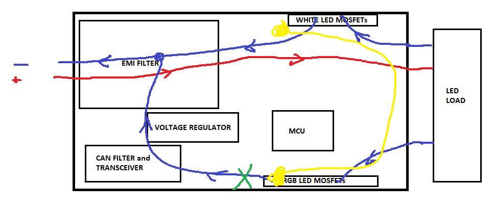
My circuit layout is like below in the 2-layer pcb card. The problem seems there is a huge current loop when the RGB LEDs MOSFETs are switching. When I cut the RGB side return path and connected it with a cable to the white side, CAN error frames are no longer received.

My circuit layout is like below in the 2-layer pcb card. The problem seems there is a huge current loop when the RGB LEDs MOSFETs are switching. When I cut the RGB side return path and connected it with a cable to the white side, CAN error frames are no longer received in normal temperature. But in high temperature medium, the error frames are continueing to be received.
In my 4 layer design, I receive the error frames in high temperature medium, not in room temperature.
The core of the problem is seems something like the temperature tollerance of the some components used in the circuit.

But very interestingly, in my 2-layer design, I have a card that works flawlessly even at high temperature.

enter image description here

\$\endgroup\$

Your Answer

By clicking “Post Your Answer”, you agree to our terms of service and acknowledge you have read our privacy policy.

Not the answer you're looking for? Browse other questions tagged or ask your own question.