2
\$\begingroup\$

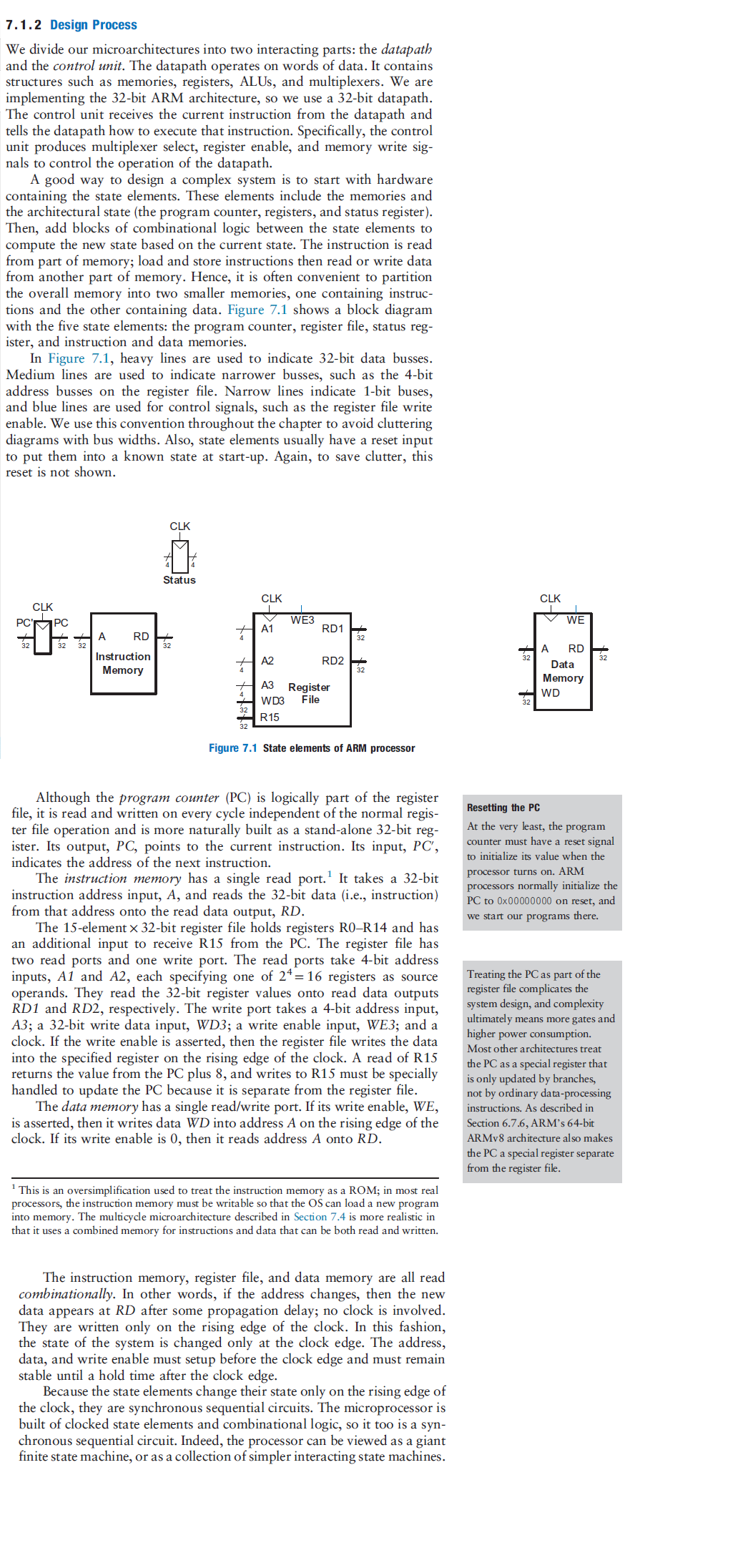
This picture is from the book Digital Design and Computer Architecture: ARM Edition. It implements the LDR instruction.

enter image description here

I have one question:

  1. R15 is supposed to be PC+8. In the picture, is R15 written on the rising edge of the clock? Because then it will only be PC+4 since it takes the current PC+8, and not PC'+8. Or have I misunderstood something?

Below is everything that is from the LDR implementation, I include it in case there are some things that are needed:

enter image description here

enter image description here

\$\endgroup\$
4
  • 2
    \$\begingroup\$ I'm not going to read everything there. But at a surface glance over the blocks and diagram, I'd hazard a guess that the R15 input has combinatorially settled down by the time a rising clock edge arrives at the Register File block and that the Register File itself doesn't actually have an internal latch for it. If a read on A1 specifies R15, it just muxes that input over to its RD1 as the output. Otherwise, it muxes over the output of the internal register file memory, which has fewer than 16 entries in it. The whole thing is conceptual, though. Keep that in mind. \$\endgroup\$
    – jonk
    Commented Aug 13, 2022 at 22:27
  • \$\begingroup\$ No problem, at all. I hope my perspective may have helped a little. I scanned over the text a little more and I still think I may be right. But I'd like your opinion, too. Do you feel I explained things in a way that does makes sense to you in the context of what you are reading and learning? (Oh, and +1 for the question itself. Lots of material to example. More than many provide in similar cases. So I was glad for that.) \$\endgroup\$
    – jonk
    Commented Aug 14, 2022 at 6:12
  • \$\begingroup\$ @jonk Yes it does make sense. From what I understood you said that R15 does not update at the clock edge, but updates after the normal delays and that solves the problem. \$\endgroup\$
    – user394334
    Commented Aug 14, 2022 at 7:32
  • \$\begingroup\$ Great. Then we share a similar perspective, I imagine! Best wishes!! I love the fact that you are getting into this stuff. It's deep in my heart. I worked at Intel on the BX chipset and still earlier developed my own MCU design as well as working with other MCUs with other designers. It's something I really do enjoy. And you are a becoming a brother of mine. You have my very best wishes! \$\endgroup\$
    – jonk
    Commented Aug 14, 2022 at 8:12

1 Answer 1

1
\$\begingroup\$

R15 is an input to the register file. In other words, it is a wire. Wires do not store any data, they merely propagate data.

R15 comes from PCPlus8. PCPlus8 = 4 + PCPlus4

As PCPlus4 = PC + 4,

R15 = PCPlus8 = 4 + (PC + 4) = PC + 8.

The adders used in the diagram for PC + 4 and PC + 8 are pure combinational circuits, hence their outputs are computed in the same cycle.

This implies R15 propagates the value of PC + 8. Any Register Reads of R15 in the same cycle that PC is input to R15 will result in PC + 8. This is assuming all setup time and hold time requirements of the design are met.

From Arm's official documentation, the R15 register holds the Program Counter Value. This means it holds the address of the next instruction to be executed, which is PC + 8, where PC denotes the current instruction being executed. The instruction that gets executed in the next cycle depends on the value of the multiplexer select line (PCSrc) that selects between R15 and PC + 4.

\$\endgroup\$

Your Answer

By clicking “Post Your Answer”, you agree to our terms of service and acknowledge you have read our privacy policy.

Not the answer you're looking for? Browse other questions tagged or ask your own question.