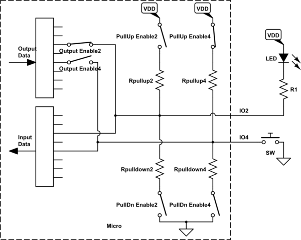
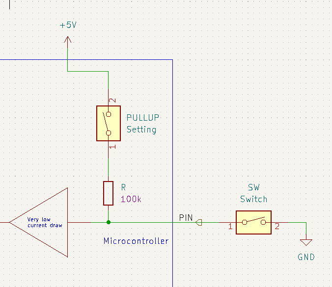
The diagram shows a standard microcontroller GPIO interface (simplified). There are variations but they are all very similar. Older microcontrollers had no pullup or pull down resistors. They had to be added externally. First the pull up resistors appeared. I remember being surprised that all were enabled at reset making all the inputs VDD. Currently many default to High-Z (all enable switches open).
The diagram displays a configuration to interface to a LED and to a push button.
IO2 is configured as an output by closing the output enable switch. You can see the path from the output data register to the IO2 pin. Notice that IO2 is still connected to the input data register. This is so that software can read the state of the pin whether it is an input or an output. Applying a 1 to the IO2 data bit in the output data register applies VDD to the LED-resistor pair. The voltage drop across the LED is zero so it if OFF. Applying a 0, grounds the pair turning the diode ON. In this case the voltage is sourced through the data register or an associated amplifier.
IO4 has its output function disabled. The output enable switch is open. Notice that I did not say it was configured as an input because all the pins are always connected as inputs. This function does not need to be configured. The output function is disabled by configuration.
The switch in its normal state is open (essentially non-existent). So, to generate a high state the associated pullup resistor is enabled. In this case VDD is applied through the pullup resistor to IO4. Since there is no path for the current to flow, then the IO4 pin will be 5v. The input data register will be 1 for that bit.
To answer your last question IO4 is an input, but it has a voltage source with a high internal resistance in parallel with the input. The pullup resistor allows the pushbutton to take over.
Closing the switch applies a voltage of 0V to IO4. This creates a path for current to flow through the pullup allowing the voltage to drop across it. Since IO4 is now 0V the associated bit in the input data register will be 0.
I leave it to you to redraw the diagram for the LED connected to ground, and the pushbutton connected tp VDD. Both layouts are valid. Interpretation by software will change. Does Light On map to 0 or 1? Does button pressed map to 0 or 1?

simulate this circuit – Schematic created using CircuitLab


