4
\$\begingroup\$

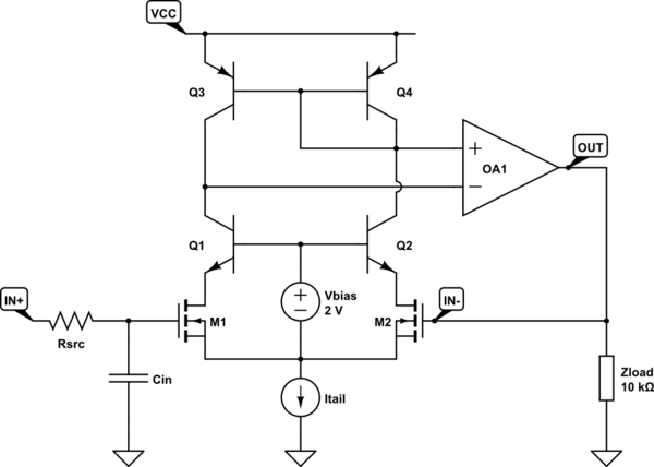
In the below schematic of a cascode-input op-amp, the input transistors M1 and M2 present no capacitive load to the input signals, because their gate-source and gate-drain voltages are stabilized. The schematic omits frequency compensation components for clarity.

schematic

simulate this circuit – Schematic created using CircuitLab

I was wondering, why modern cascode-input op-amps still exhibit an input capacitance on the order of 5 pF for general purpose parts.

When I simulate the above-mentioned op-amp structure in a voltage follower application (approx. as drawn), I first use Cin = 0 and Rsrc = 0, i.e. I do not include any additional input capacitance and source impedance. It works as expected, and the observable input capacitance (e.g in time domain analysis) turns out to be negligible \$\ll\$1 pF.

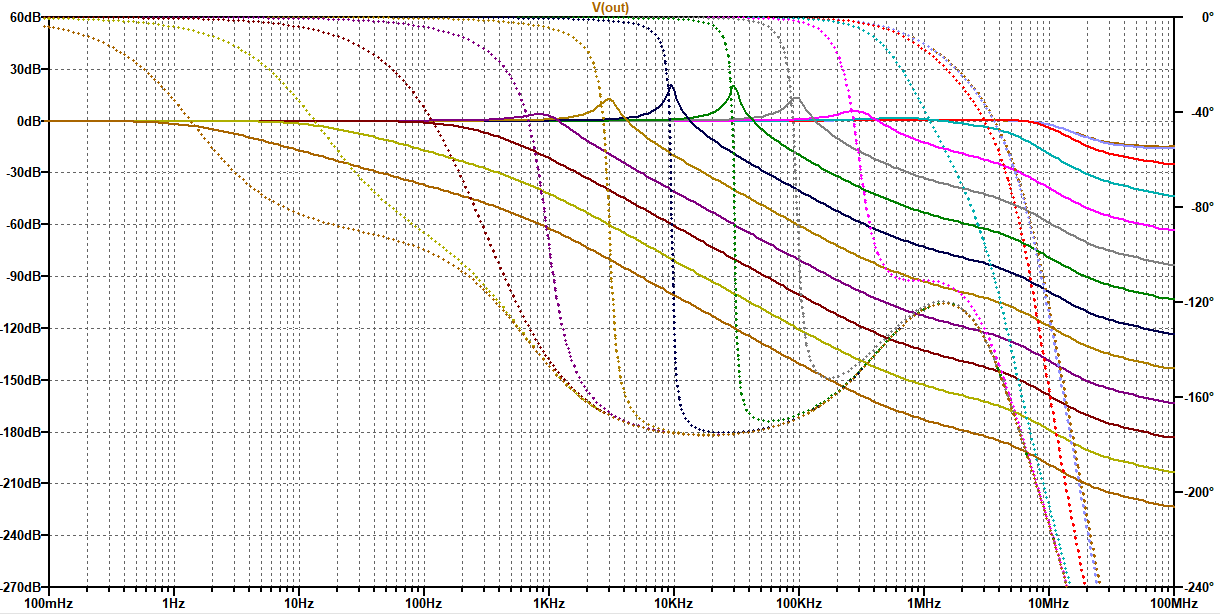
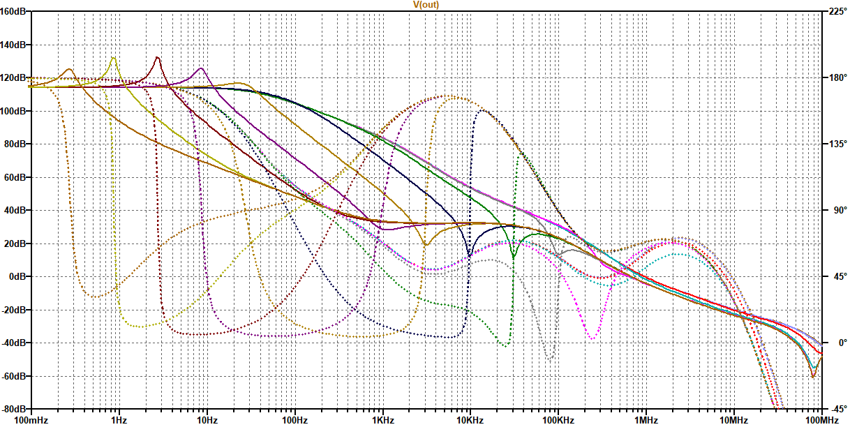
Next, I included the source impedance. It continues to work well if Rsrc is very small (<1 kΩ) or very large (>1 GΩ). But I observe strong positive feedback and gain peaking for intermediate values of Rsrc like 1 MΩ. The peak frequency is in the kHz range and scales with \$\propto 1/\sqrt{R_\text{src}}\$. The plots below show closed-loop gain and open-loop gain for source resistances from 1 TΩ (left) to 1 Ω (right).

enter image description here enter image description here

If I then also include a Cin = 5 pF, the gain peaking seems to be well controlled, at the expense of some input bandwidth.

Questions:

  1. Why do modern cascode-input op amps have such large Cin? Is it left deliberately because it is the only/simplest way to stabilize these op-amps for voltage follower application ?

  2. Without Cin, there is gain peaking/ringing for intermediate frequencies and intermediate source impedances: How does it come about? I have trouble identifying the responsible pole (at about 1 kHz) and which circuit part gives rise to it.

\$\endgroup\$
7
  • \$\begingroup\$ When used differentially they do present input capacitance because the common source node has very little AC signal on it and, it can be regarded as being at a fixed DC value of voltage. Is this what you are driving at? \$\endgroup\$
    – Andy aka
    Commented Oct 5, 2022 at 11:21
  • \$\begingroup\$ @Andyaka I am not sure I understand your question. In the voltage follower application, both inputs move in tandem and also in common with the common-source node, which therefore sees the full AC voltage. I believe (in terms of opamp spec sheets) this is called the common-mode input impedance, which usually is on the order of 5 pF for FET op-amps. \$\endgroup\$
    – tobalt
    Commented Oct 5, 2022 at 11:36
  • \$\begingroup\$ I mentioned this because your question is: Why do modern cascode-input opamps have such large Cin <-- and this is because it will be a general value (not assuming that it is acting as a voltage follower). \$\endgroup\$
    – Andy aka
    Commented Oct 5, 2022 at 12:04
  • \$\begingroup\$ @Andyaka but spec sheets give the input capacitance for both cases: differential input and common input. If Cin wasnt present, I would expect the common-mode input capacitance to be <<1pF, but it is usually the same value as the differential-mode input capacitance. \$\endgroup\$
    – tobalt
    Commented Oct 5, 2022 at 12:10
  • \$\begingroup\$ I would think that's more of a representative model to give meaning to the characterization parameters rather than the circuit actually being intentionally built with those components there. \$\endgroup\$
    – DKNguyen
    Commented Oct 10, 2022 at 5:42

1 Answer 1

2
+250
\$\begingroup\$

In my experience, I have never seen anyone place an explicit capacitor at the input of an op-amp for stabilization purposes. As DKNguyen commented, this is more of a representative model of the amplifier rather the actual implementation.

Also, 5pF is quite small!

The value of this input capacitance is, most likely, a sum of several contributors, such as:

  1. Internal compensation capacitor. If it's a miller compensation cap, it'll appear at the input scaled-up by a gain factor.

  2. The input stages of most amplifiers is sized with a very big multiplication factor (think m_factor*W/L of your input stage transistor sizes) as you want to boost your gm and, thus, lower your input-referred shot noise. This has 2 consequences: 1/f noise will be reduced due to less charges being trapped and de-trapped, and, finally, your input capacitance at the gate (think gate-to-source cap and the gate-to-drain as well) will be increased for the very reason that your gate-oxide area is larger (distances between plates remain the same). Another reason for a large input stage is because of matching. Larger area, less mismatch variation.

  3. As Tim williams also added, the ESD transistors will also contribute an input capacitance. The ugly part of these components is that their caps are non-linear, thus will contribute to distortion, specially at high input levels (i.e. when they're relatively close to being triggered)

To answer your question, then:

  1. Fundamentally, a large Cin is a consequence of the frequency compensation measures to keep the amplifier stable. In addition to the noise, ESD and matching considerations at the input.

For 2), it's more complicated to answer without any more details.

I think it's very difficult to say without plots and loop gain responses why you're getting so much instability with a "middle-valued" input resistance. I can only speculate: perhaps, if it's small, your pole is at very high-frequency beyond your unity-gain frequency, and if it's too big, then you're moving it too close, as sort-of-a poor man's dominant pole compensation, but now your dominant pole is in the closed loop, and it overrides your loop gain because the time-constant is so large.

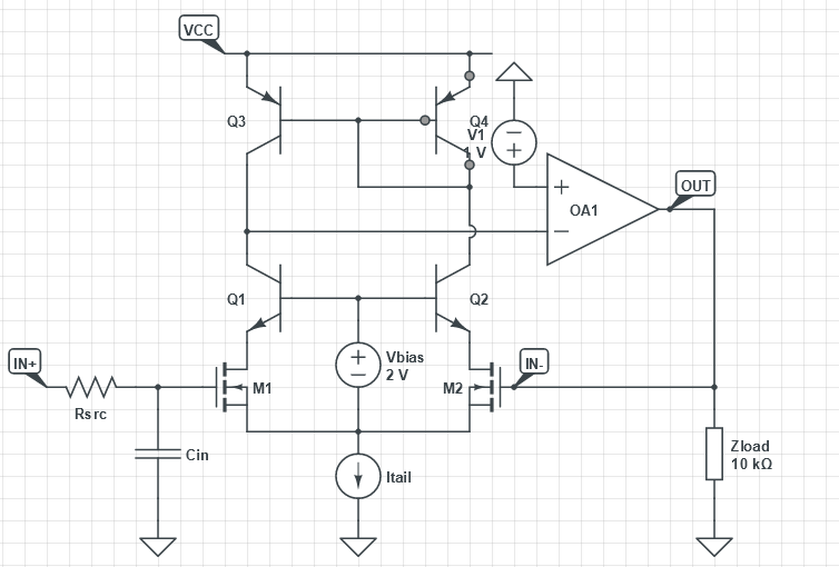
Finally, could you argument why did you connect your cascode input-stage to the op-amp like that? From a first look, it doesn't seem like a good idea. You have a forced a single-ended amplifier into a differential one. Between Q4 and Q2, the swing should be pretty small as you're mostly diverting the current to left side. However, now you have slowed-down that node as it must charge OA1+ terminal now. Certainly contributes to your frequency response.

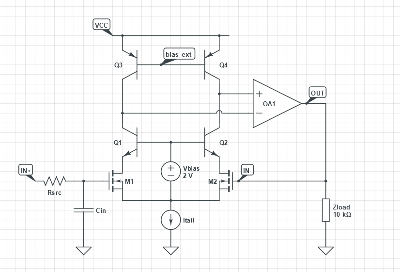
If I really wanted to connect the input stage differential output to the op-amp, I'd generate the bias voltages for Q3 and Q4 bases elsewhere, and then connect both outputs as you've done. Otherwise, disconnect QA1+ and fix it to a DC voltage.

Sorry for the screenshots, they were asking me for a subscription to save the circuits...

Single-ended input-stage connection Single-ended input-stage connection
Differential-connection input-stage. Vbias_ext generated elsewhere Differential-connection input-stage. Vbias_ext generated elsewhere
EDIT: REWRITTEN

I should've paid attention to the title of your plots. The definition of open-loop gain is V(out)/(Vin+ - Vin-). If you plot that, sure enough, you get that the open-loop response is independent of any source resistance you pick.

https://i.sstatic.net/uSIzo.jpg

If you look at the loop gain V(out)/V(in-), then you'll find that the dominant pole of your loop is a function of your source resistance, obviously. I withdraw what I edited previously, there's instability, indeed, at 100kohm resistance.

While an analysis of your design is quite involved because you're using a bootstrapped cascode, I can tell you that a lot more is affected by your dominant pole due to the output resistance of your differential pair seeing the input cpi and cbc of the cascodes.

In order to verify it, I simplified your schematic to this:

https://i.sstatic.net/uy5Re.jpg

I kept getting no phase margin for Rsrc=100kohm.

https://i.sstatic.net/v4HiF.jpg

As I said before, I suspected the bootstrapped nodes from your bottom current source, through the 22k to the cascode bases.

So, I removed the bootstrapping and just kept the biasing of the cascode with a fixed voltage source:

https://i.sstatic.net/ZsWMI.jpg

Then, I see that the notch in your loop gain is moved upwards. We have decoupled the source of your diff pair and the cascode.

https://i.sstatic.net/FMasE.jpg

If you must use the bootstrapping for either reason, then, adding an RC shunt at the gate of those gate nodes might help. I tried with 1kohm and 100pF, and the notch is moved to a higher frequency.

https://i.sstatic.net/O5nNB.jpg

To summarize, any designer MUST always know his input source impedance before starting any design. Doesn't matter if it's not constant, you must know its bounds before starting any design.

Good luck with your design going forward!
\$\endgroup\$
10
  • \$\begingroup\$ Thanks, Ernesto! I have added the loop gain plot to the question. The pole frequency seems to be rather constant at about 1 kHz, but the gain peak scales with Rsrc. About that op-amp connection: I guess that your first image is infact equivalent to the circuit in my question. The bias is generated by the diode-connected transistor Q4. This bias is perfect to keep Q3 well within its active region. \$\endgroup\$
    – tobalt
    Commented Oct 10, 2022 at 10:03
  • \$\begingroup\$ @tobalt , I didn't say it wouldn't work, but that it's not a good idea, though I have no idea what kind of amplifier you're trying to achieve. Such a connection would add an extra slow time constant into your loop gain, as there's signal present in that node. I'd argue my schm and yours are not equivalent. You have now coupled biasing with signal in that node. Whether that's good enough for your purposes, I wouldn't know. Will check out your plots later. \$\endgroup\$
    – Designalog
    Commented Oct 10, 2022 at 10:09
  • \$\begingroup\$ I also tried the other two biasing methods, but the results are indifferent. I tried changing the miller capacitance (which is wrapped around the OA1). And this will indeed move the pole frequency proportionately to higher/lower frequencies but doesn't seem to have an effect on the amplitude of the gain peak. \$\endgroup\$
    – tobalt
    Commented Oct 10, 2022 at 10:17
  • 1
    \$\begingroup\$ Let us continue this discussion in chat. \$\endgroup\$
    – Designalog
    Commented Oct 10, 2022 at 11:09
  • 1
    \$\begingroup\$ @tobalt I took a closer look at your amplifier and found that, most likely, that instability is coming from an extra pole in your circuit caused by the bootstrapped cascode you're using. I couldn't upload any image, so I provided imgur links. Adding an "RC damper" fixed the problem. \$\endgroup\$
    – Designalog
    Commented Oct 15, 2022 at 12:05

Your Answer

By clicking “Post Your Answer”, you agree to our terms of service and acknowledge you have read our privacy policy.

Not the answer you're looking for? Browse other questions tagged or ask your own question.